Light-emitting diode and vehicular lamp

Active Publication Date: 2007-02-08
KOITO MFG CO LTD
23 Cites 93 Cited by

AI-Extracted Technical Summary

Problems solved by technology

This, however, causes problems that such a light-emitting diode cannot radiate light with sufficient luminance in an oblique direction while the light-emitting diode radiates light with sufficient luminance in the forward direction.
When such light-emitting diodes as described above are used as a light source of a vehicular lamp, several problems occur.
However, when a light-emitting diode is used as a light source, such a lens arrangement cannot sufficiently mitigate the sharp luminance distribution of the light-emitting diode.
As a res...

Method used

[0082] If it is assumed that the curved surface portion 14aA of the sealing member 14 have an outer shape of a horizontally bilobal shape that extends in the lateral direction with a uniform width in the vertical cross-section which is the same as that in the vertical plane shown in FIG. 10A, then only the light emitted from the light-emitting chip 12 in the direction within the angle range of γ2′ (γ2′<γ2) would reach the curved surface portion 14aA′ indicated by the line of alternating one long and two short dashes, resulting in that the luminous flux utilization factor with respect to the light emitted from the light-emitting chip 12 is reduced. However, in the shown embodiment, the curved surface portion 14aA of the sealing member 14 is formed so that the outer shape is a horizontally bilobal shape that has a transversely narrowed part in the middle in the longitudinal direction of the bilobal outer shape. Accordingly, the luminous flux utilization factor with respect to the light emitted from the light-emitting chip 12 improves.
[0086] Furthermore,...

Benefits of technology

[0027] In the present invention, the perimeter of the curved surface portion of the front face of the sealing member can be formed with a deflection directing portion, which directs the light emitted from the light-emitting chip so that it is deflected toward the optical axis. This structure improves the utilization efficiency for the light emitted from the light-emitting chip.
[0028] In particular, in a case that the cross-sectional shape of the curved surface portion of the sealing member taken along the second plane is in a shape of a convex curve, a relatively large...

Abstract

A light-emitting diode including a curved surface portion 14aA formed in the front face of a sealing member 14 with the cross-sectional shape of the curved surface portion being in the shape of an undulating curve that has a concave curve C1 near the optical axis and convex curves C2 on both sides of concave curve C1, thus allowing the light emitted from a light-emitting chip 12 at a small divergence angle centered on the optical axis Ax to reach the concave curve C1 and to be directed forward as diffused light deflected from the optical axis and further allowing the light emitted at a large divergence angle centered on the optical axis Ax to reach the convex curves C2 and to be directed forward as light deflected toward line L positioned at the divergence angle θ.

Application Domain

Technology Topic

Image

  • Light-emitting diode and vehicular lamp
  • Light-emitting diode and vehicular lamp
  • Light-emitting diode and vehicular lamp

Examples

  • Experimental program(4)

Example

[0049] The first embodiment of the present invention will be described first.
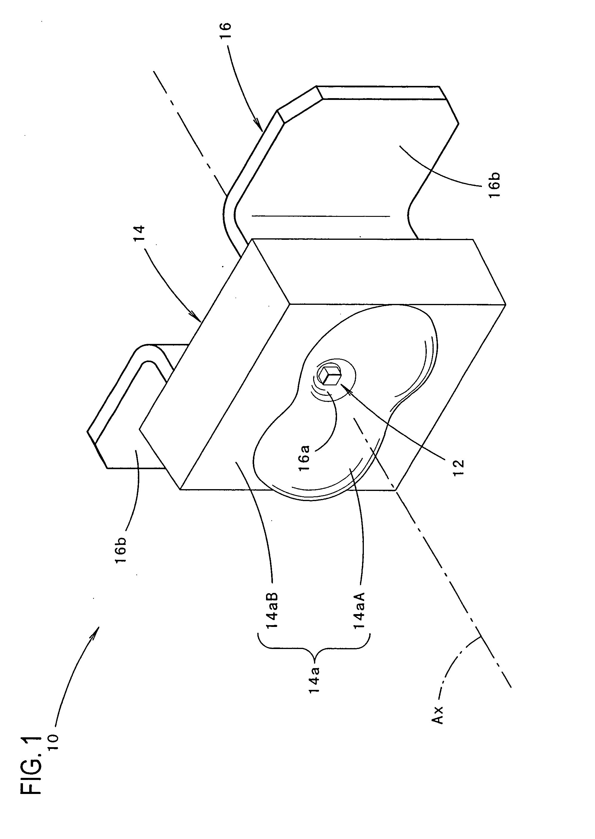
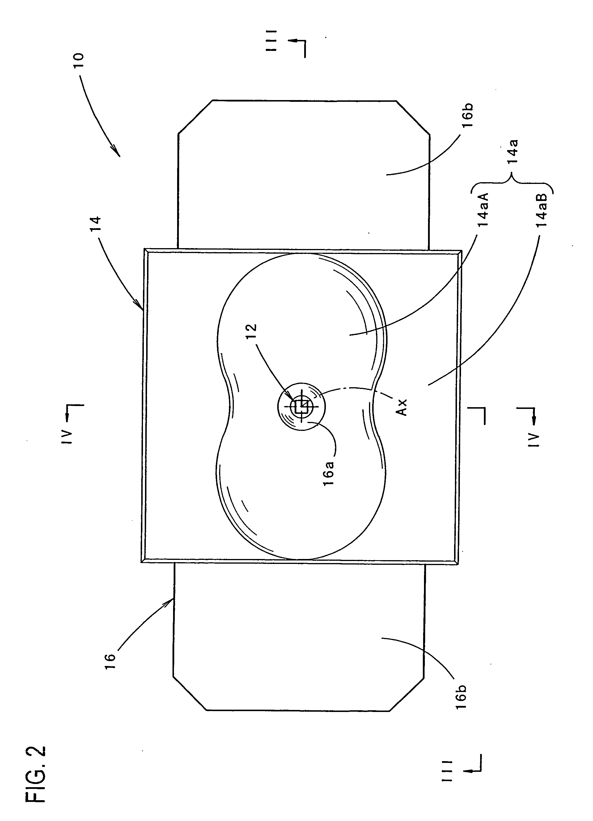
[0050]FIG. 1 is a perspective view of the light-emitting diode 10 according to the first embodiment, and FIG. 2 is a front view thereof. FIG. 3 and FIG. 4 are the cross-sectional views taken along the line III-III and line IV-IV in FIG. 2, respectively.
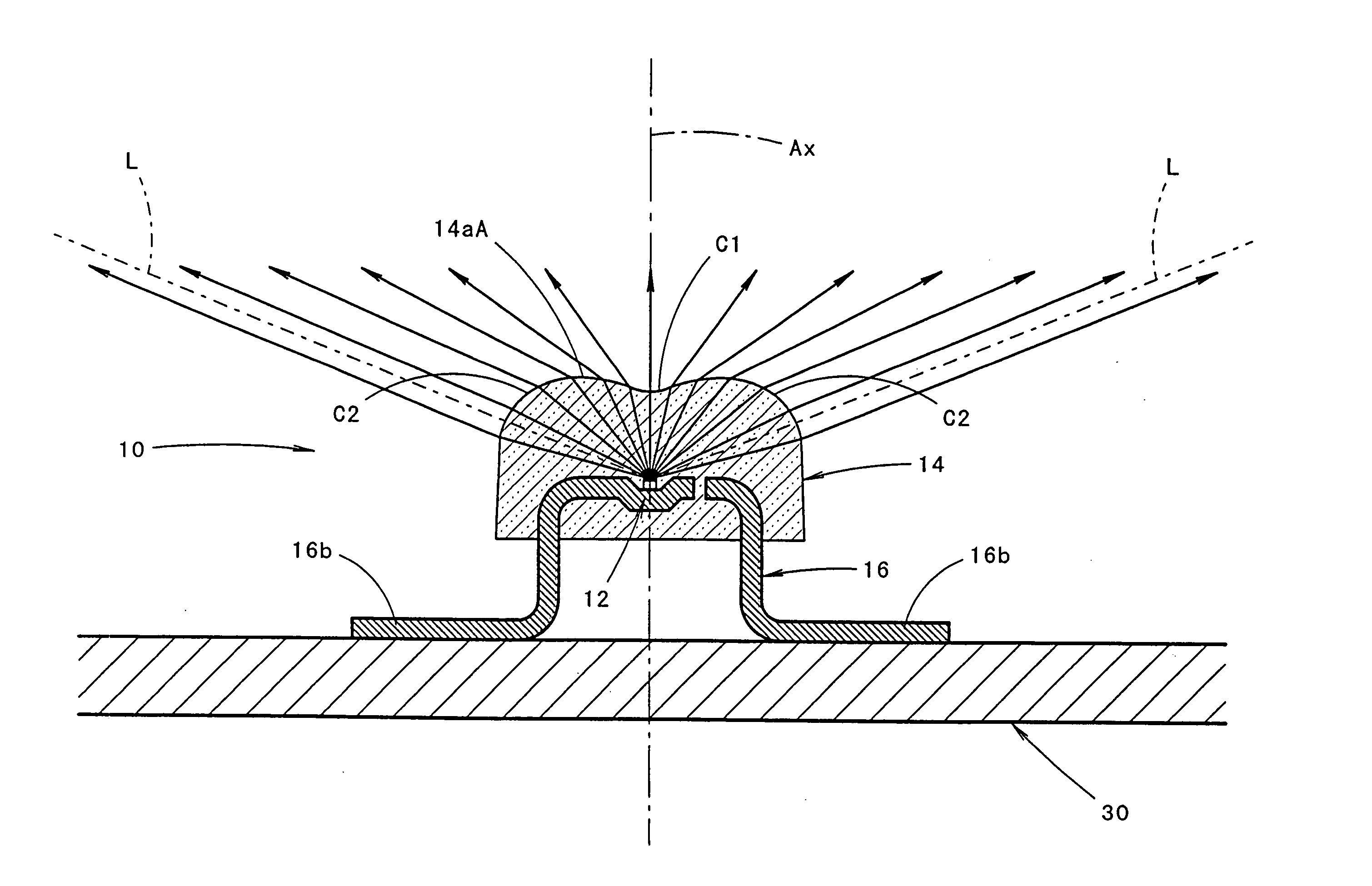
[0051] As seen from FIGS. 1 through 4, the light-emitting diode 10 is comprised of a light-emitting chip 12 disposed on a predetermined optical axis Ax, a transparent sealing member 14 that seals the light-emitting chip 12 on the side that faces the forward direction along the optical axis Ax (which will simply be referred to as “front side” hereafter), and a lead frame 16 for supporting the light-emitting chip 12.
[0052] The light-emitting chip 12 has a light emitting face of around 0.3 to 1 mm square and is disposed with its light emission center O positioned on the optical axis Ax and with its light emitting face facing toward the front face (i.e., in the forward direction along the optical axis Ax).
[0053] The sealing member 14 is made of a transparent resin such as epoxy resin or the like and is formed square in its outer shape when viewed from the front. The depth of the sealing member 14 is about half the length of one side of its square shape. The sealing member 14 seals the light-emitting chip 12 and a part of the lead frame 16, so that the sealing member 14 wraps around the rear face of the light-emitting chip 12.
[0054] The front face 14a of the sealing member 14 has a flat surface portion 14aB, which is formed along the vertical plane orthogonal to the optical axis Ax, and a curved surface portion 14aA, which is formed in a shape of two humps that protrude forward from the flat surface portion 14aB.
[0055] As shown in FIG. 3, the cross-sectional shape of the curved surface portion 14aA taken along the horizontal plane that includes the optical axis Ax is formed by an undulating curve that has a concave curve C1 positioned near the optical axis Ax and convex curves C2 on both left and right sides of the concave curve C1.
[0056] The shape of this undulating curve is bilaterally symmetrical with respect to the optical axis Ax. The concave curve C1 is formed over the range of a central angle in an angle range of around 15 to 25° (e.g., around 20°) with the light emission center O of the light-emitting chip 12 as a reference point. Each of the convex curves C2 is formed over the range of the above-described central angle in an angle range of around 60 to 70° (e.g., around 65°).
[0057] As seen from FIG. 3, the concave curve C1 is formed in a shape of an arc having a relatively large curvature. On the other hand, each of the convex curves C2 is formed with a gradually changing curvature. More specifically, each of the convex curves C2 is formed so that it has the same curvature as the curvature of the concave curve C1 at positions where the concave curve C1 is coupled with the convex curves C2, thus allowing the concave curve C1 and each of the convex curves C2 to be connected with one another. Furthermore, each of the convex curves C2 is formed with a curvature that gradually decreases according to the increase in the divergence angle centered on the optical axis Ax in the lateral direction. In this arrangement, each of the curves C2 is formed so that its smallest curvature is at a position over the angle θ (direction denoted by the line L of alternating long and short dashes in FIG 3) which is somewhat smaller than the far edge divergence angle (i.e., α/2+β). Furthermore, the arc of each of the curves C2 has a constant curvature at the above-described divergence angle or more. The divergence angle θ is set to be around 65 to 75° (e.g., around 70°).
[0058] On the other hand, as seen from FIG. 4, the cross-sectional shape of the curved surface portion 14aA taken along the vertical plane, which is parallel to the optical axis Ax, is formed by a convex curve C3. The convex curve C3 is formed by an arc, which has its minimum radius on the optical axis Ax, and the radius of the convex curve C3 then gradually increases as the distance from the optical axis Ax in the lateral direction increases. The radius of the convex curve C3 then gradually decreases pursuant to the further increase in the distance from the optical axis Ax in the lateral direction. The center of the arc that forms the convex curve C3 is positioned somewhat forward with respect to the light emission center O of the light-emitting chip 12.
[0059] Since the horizontal cross-sectional shape and the vertical cross-sectional shape of the curved surface portion 14aA take curves as described above, the curved surface portion 14aA has a horizontally bilobal outer shape that has a transversely narrowed part at the middle portion in the longitudinal direction of the bilobal outer shape when viewed from the front.
[0060] The lead frame 16 has, as seen from FIG. 3, a shape that it is formed by bending a belt-shaped metal plate into an inverted letter-U shape and then by further bending both ends at right angles so that they extend in the directions opposite to one another. The light-emitting chip 12 is provided at the center of the upper level portion (or of the bottom of the U) of the lead frame 16. A cone-shaped recess 16a is formed at the center of the upper level portion of the lead frame 16, and the light-emitting chip 12 is provided in the center of the bottom of the recess 16a. As best seen from FIG. 5, the lead frame 16 is comprised of left and right separated parts, which are separated in the upper level portion. The light-emitting chip 12 is mounted on one of these separated parts (which is the left side part in FIG. 5), and bonding wires (not shown) extending from the light-emitting chip 12 are connected to the other part (which is the right side part in FIG. 5). While the upper level portion of the lead frame 16 and the light-emitting chip 12 are sealed by the sealing member 14 as described above, a part of each of the pair of left and right terminals 16b of the lead frame 16 extends out of the sealing member 14.
[0061] As shown as a plane (horizontal) cross-sectional view in FIG. 5, the light-emitting element 10 is provided, at both terminals 16b of the lead frame 16, on the support board 30.
[0062] Next, the advantages of the first embodiment will be described.
[0063] As shown in FIG. 5, a part of the light emitted by the light-emitting chip 12, which has been emitted at a small divergence angle centered on the optical axis Ax in the lateral direction in a horizontal plane that includes the optical axis Ax, reaches the area of the concave curve C1 of the curved surface portion 14aA. Accordingly, such light is directed forward and diffused so that it is distanced from the optical axis Ax by the light-diffusing function of the concave curve C1 of the curved surface portion 14aA. On the other hand, a part of the light emitted by the light-emitting chip 12, which has been emitted at a wide divergence angle centered on the optical axis Ax in the lateral direction, reaches the areas of the convex curves C2 of the curved surface portion 14aA. Accordingly, such light is directed forward so that it is deflected toward lines L positioned at the divergence angle θ with respect to the optical axis Ax by the light convergence function of the convex curves C2 of the curved surface portion 14aA.
[0064]FIGS. 6A and 6B show the luminance distributions of the light-emitting chip 12 within the horizontal plane that includes the optical axis Ax. In particular, FIG. 6A shows a luminance distribution of the light emitted from the light-emitting chip 12. FIG. 6B shows a luminance distribution of the light directed from the curved surface portion 14aA of the sealing member 14 after the emission from the light-emitting chip 12.
[0065] As seen from FIG. 6A, the luminance distribution of the light emitted from the light-emitting chip 12 exhibits the maximum luminance on the optical axis Ax extending in the forward direction. Furthermore, it is a characteristic of this luminance distribution that the luminance rapidly decreases according to the increase in the divergence angle centered on the optical axis Ax. This is because the light-emitting chip 12 is disposed so that the light-emitting face faces forward.
[0066] On the other hand, as seen from FIG. 6B, the luminance distribution of the light directed from the curved surface portion 14aA of the sealing member 14 has a shape that is similar to a suspension bridge. In other words, it is a characteristic of this luminance distribution that the maximum luminance value appears in the direction over a divergence angle, which is somewhat smaller than the divergence angle θ, centered on the optical axis Ax in the lateral direction. Furthermore, in this luminance distribution, the luminance decreases according to the reduction in the divergence angle from the above-described divergence angle and exhibits its minimum value on the optical axis Ax. On the other hand, the luminance rapidly decreases according to the increase in the divergence angle beyond the divergence angle θ. This is because the cross-sectional shape of the curved surface portion 14aA, which is taken along the horizontal plane that includes the optical axis Ax, includes the undulating curve formed by the concave curve C1 positioned near the optical axis Ax and the convex curves C2 positioned on the left and right sides of the concave curve C1.
[0067] As seen from the above, the light-emitting diode 10 of the first embodiment of the present invention has no such a problem of conventional light-emitting diodes in which a rapid reduction in luminance occurs as the divergence angle with respect to the optical axis increases.
[0068] Furthermore, in the above-described light-emitting element 10, the cross-sectional shape of the curved surface portion 14aA of the sealing member 14 taken along the vertical plane that is parallel to the optical axis Ax has the convex curve C3. Accordingly, the luminance distribution of light emitted by the light-emitting chip 12 and directed from the curved surface portion 14aA of the sealing member 14 takes a luminance distribution that is created by concentrating the luminance distribution of the light, which has been emitted by the light-emitting chip 12, within a predetermined angle range of a small divergence angle centered on the optical axis in the vertical direction.
[0069] Furthermore, in the light-emitting diode 10 of the first embodiment, the concave curve C1 and each of the convex curves C2 positioned on the left and right sides of the concave curve C1 (the concave curve C1 and the convex curves C2 forming the cross-sectional shape of the curved surface portion 14aA of the sealing member 14 taken along the horizontal plane that includes the optical axis Ax) are connected (or in continuous) smoothly with one another. Accordingly, the luminance distribution of the light that is directed from the curved surface portion 14aA of the sealing member 14 changes smoothly.
[0070]FIG. 7 and FIG. 8 show, in plane (horizontal) cross-section and in side (vertical) cross-section, respectively, the vehicular lamp 50 that is installed with the light-emitting diode 10 of the first embodiment as its light source.
[0071] As seen from FIGS. 7 and 8, the vehicular lamp 50 includes: a polygonal lamp body 32 for fixing the support board 30, which supports and fixes the light-emitting diode 10, at its perimeter portion; an inner lens 34, which is fixed at a front end opening 32a of the lamp body 32; and an outer lens 36, which is fixed to the lamp body 32 with the inner lens 34 pressed in contact with the front end opening 32a of the lamp body 32.
[0072] The vehicular lamp 50 has an outer shape of a horizontally long rectangle with a smaller vertical width (height) when viewed from the front. More specifically, the horizontal width of the vehicular lamp 50 is set to be a value around four times greater than the vertical width (height). Thus, the support board 30, the inner lens 34 and the outer lens 36 are formed accordingly in the shape of a horizontally long rectangle. The lamp body 32 is in the shape of a polygon that has a rectangular cross-sectional shape along the vertical plane orthogonal to the optical axis Ax.
[0073] The rear face 34a of the inner lens 34 has, as seen from FIG. 9, a cylindrical surface that extends in its lateral direction. The convex curve C4, which forms the cross-sectional shape taken along each vertical plane parallel to the optical axis Ax, is formed by an arc having a predetermined curvature that gradually reduces according to the increase in the distance from the optical axis Ax in the lateral direction. Furthermore, the cross-sectional shape of the cylindrical face taken along the horizontal plane takes a gentle V-shape that gradually extends forward according to the increase in the distance from the optical axis Ax in the lateral direction.
[0074] Furthermore, the inner lens 34 has multiple prism-shaped lens elements 34s formed on the front face 34b in a shape of a stripe-shaped array having a sawtooth-shaped cross-sectional shape. The lens elements 34s cause the light incident on the inner lens 34 from the light-emitting element 10 to be deflected and directed in a direction closer to the optical axis Ax with respect to the lateral direction.
[0075] The inner lens 34 has a pair of lateral tabs 34c on the left and right sides of the outer edge and a pair of longitudinal tabs 34d on its upper and lower edges. The inner lens 34 is fixed to the lamp body 32 with the tabs 34c and 34d aligned with the front end opening 32a of the lamp body 32.
[0076] The inner lens 34 causes light emitted from the light-emitting element 10 to be directed forward parallel to the optical axis Ax. A detailed configuration thereof will be described later.
[0077] As shown in FIG. 7 and FIG. 8, the outer lens 36 has multiple fisheye-lens-shaped diffusion lens elements 36s formed on the inner face. The diffusion lens elements 36s direct the light, which has been incident on the outer lens 36 from the inner lens 34 in the form of parallel light fluxes, forward from the outer lens 36 so that it is diffused in the vertical direction and the horizontal direction.
[0078]FIG. 10A is a cross-section taken along the line Xa-Xa in FIG. 7, and FIG. 10B is a cross-section taken along the line Xb-Xb in FIG. 7.
[0079] As seen from FIG. 10A, in the vertical plane that includes the optical axis Ax, the light, which has been emitted by the light-emitting chip 12 in the direction within the range of the angle γ1 centered on the optical axis Ax, is directed forward from the curved surface portion 14aA of the sealing member 14. On the other hand, as seen from FIG. 10B, in the vertical plane, which passes through the light emission center O of the light-emitting chip 12 and inclines in the lateral direction with respect to the optical axis Ax, the light, which has been emitted by the light-emitting chip 12 in the direction within the range of the angle γ2 centered on the optical axis Ax, is directed forward from the curved surface portion 14aA of the sealing member 14. The curved surface portion 14aA is formed in the shape of two humps so as to have the bilobal outer shape whose longer axis is horizontal and that has a transversely narrowed part in the middle in the longitudinal direction of the bilobal outer shape when viewed from the front. Accordingly, the angles γ1 and γ2 are set to be substantially the same value.
[0080] On the other hand, in the vertical plane shown in FIG. 10B, the convex curve C5, which forms the vertical cross-sectional shape of the curved surface portion 14aA of the sealing member 14, matches the shape obtained not only by simply enlarging the convex curve C3, which forms the vertical cross-sectional shape of the curved surface portion 14aA in the vertical plane shown in FIG. 10A, but also by slightly extending the convex curve C3 in the front-back direction. As a result, the refracting power is high with respect to the light emitted from the light-emitting chip 12. Accordingly, although the distance from the light-emitting diode 10 to the inner lens 34 in the vertical plane shown in FIG. 10B is greater than that in the vertical plane shown in FIG. 10A, such light emitted from the light-emitting diode 10 can reach the inner lens 34 without any loss.
[0081]FIG. 11A shows a cross-section taken along the line Xb-Xb in FIG. 7 in the same way as in FIG. 10B, and it is a diagram for describing the effects of the outer shape of the curved surface portion 14aA of the sealing member 14 having a horizontally bilobal shape that has a transversely narrowed part in the middle in the longitudinal direction of the bilobal shape when viewed from the front.
[0082] If it is assumed that the curved surface portion 14aA of the sealing member 14 have an outer shape of a horizontally bilobal shape that extends in the lateral direction with a uniform width in the vertical cross-section which is the same as that in the vertical plane shown in FIG. 10A, then only the light emitted from the light-emitting chip 12 in the direction within the angle range of γ2′ (γ2′ 2) would reach the curved surface portion 14aA′ indicated by the line of alternating one long and two short dashes, resulting in that the luminous flux utilization factor with respect to the light emitted from the light-emitting chip 12 is reduced. However, in the shown embodiment, the curved surface portion 14aA of the sealing member 14 is formed so that the outer shape is a horizontally bilobal shape that has a transversely narrowed part in the middle in the longitudinal direction of the bilobal outer shape. Accordingly, the luminous flux utilization factor with respect to the light emitted from the light-emitting chip 12 improves.
[0083]FIG. 11B shows a cross-section taken along the line Xb-Xb in FIG. 7 in the same way as in FIG. 10B, and it is a diagram describing the effects of the convex curve C4, which forms the cross-sectional shape of the cylindrical face forming the rear face 34a of the inner lens 34 taken along a vertical plane parallel to the optical axis Ax, with a predetermined curvature that gradually reduces according to the increase in the distance from the optical axis Ax in the lateral direction.
[0084] If it is assumed that the above-described convex curve C4 be formed with a uniform curvature as indicated by the line of alternating one long and two short dashes in FIG. 11B, then the cross-sectional shape of the rear face 34a′ of the inner lens 34 taken along the vertical plane would match the convex curve that has an increased curvature as if it is created by extending the convex curve C4 in the front-back direction, causing the refracting power to be excessive in the rear face 34a′ of the inner lens 34. Accordingly, the light cannot be directed from the inner lens 34 parallel to the optical axis Ax. However, in the shown embodiment, the convex curve C4 is formed with the curvature that gradually reduces according to the increase in the distance from the optical axis Ax in the lateral direction. Accordingly, the light to be directed from the inner lens 34 is parallel to the optical axis Ax regardless of where the light is incident on the inner lens 34.
[0085] As can be understood from the above, the entire region of the inner lens 34 appears to be illuminated at a substantially uniform luminance when the vehicular lamp 50 is observed from a position in front of the lamp in a state in which the light-emitting diode 10 is turned on without the outer lens 36. Accordingly, in a state that the outer lens 36 is added to, the entire region of the outer lens 36 appears to be illuminated at a substantially uniform luminance when the vehicular lamp 50 is observed not only from a position just in front of the lamp but also from a side position which is deviated somewhat obliquely from the front position in either the vertical or horizontal direction.
[0086] Furthermore, with regard to the inner lens 34, the cylindrical face, which forms the rear face 34a, is formed in a V-shaped cross-sectional shape taken along the horizontal plane, which gradually extends forward according to the increase in the distance from the optical axis Ax in the lateral direction. Accordingly, the light emitted from the light-emitting diode 10 is greatly refracted in the direction closer to the optical axis Ax by the rear face 34a of the inner lens 34, allowing the light to be directed from the inner lens 34 in parallel to the optical axis Ax, thus improving the light directing efficiency of the multiple prism-shaped lens elements 34s formed on the front face 34b.
[0087] Though in the above-described vehicular lamp 50 the parallel light is diffused in the vertical direction and the lateral direction by the outer lens 36 after the light emitted from the light-emitting element 10 is adjusted so as to be parallel light fluxes, other arrangements are possible so that the front face of the inner lens 34 has such a diffusion function as described above while the outer lens 36 has a plain lens function and so that the outer lens 36 is omitted. Next, the second embodiment according to the present invention will be described.
[0088]FIG. 12 is a perspective view of the light-emitting diode 110 of the second embodiment, and FIG. 13 is a front view thereof FIG. 14 and FIG. 15 are cross-sectional views taken along the line XIV-XIV and line XV-XV in FIG. 13, respectively.
[0089] As seen from FIGS. 12 through 15, the light-emitting diode 110 has the same basic configuration as that of the light-emitting diode 10 of the above-described first embodiment. The configuration of the front face 114a of the sealing member 114 of the light-emitting diode 110, however, differs from that of the first embodiment.
[0090] In other words, the front face 114a of the sealing member 114 is formed by a curved surface portion 114aA and a deflection directing portion 114aB.
[0091] The curved surface portion 114aA has entirely the same structure as that of the curved surface portion 14aA of the front face 14a in the sealing member 14 of the first embodiment.
[0092] The deflection directing portion 114aB of the sealing member 114 has a shape created by dividing the flat surface portion 14aB of the front face 14a of the sealing member 14 of the first embodiment in the form of a series of concentric circles, and by protruding these divided parts forward in a stepped manner so as to have a sawtooth-shape in cross-section. Each of the circular stepped portions 124, which form the deflection directing portion 114aB, has an inside sloped portion 124A and an outside sloped portion 124B. The inside sloped portion 124A has a conical face which is shifted in the forward direction and toward the outer side in the radial direction with respect to the optical axis Ax. The outside sloped portion 124B has a conical face created by slightly and gradually reducing the diameter of cylindrical face in the forward direction with the optical axis Ax as the center. The deflection directing portion 114aB is formed so that the light emitted from the light-emitting chip 12 and reached the deflection directing portion 114aB is directed at the outside sloped portion 124B in such a manner that it is deflected toward the optical axis Ax.

Example

[0093] The light-emitting diode 110 of the second embodiment has the same advantages as those of the light-emitting diode 10 of the first embodiment, and it further improves the utilization efficiency for the light emitted from the light-emitting chip 12.
[0094] In particular, the light-emitting diode 110 of the second embodiment has the curved surface portion 114aA in the front face 114a of the sealing member 114, and this curved surface portion 114aA has an outer shape of horizontally bilobal shape a transversely narrowed part in the middle in the longitudinal direction of the bilobal outer shape when viewed from the front. Accordingly, a considerable amount of light emitted from the light-emitting chip 12 is directed toward the deflection directing portion 114aB, and it is markedly advantageous to take the configuration of the second embodiment.

Example

[0095] Next, the third embodiment of the present invention will be described below.
[0096]FIG. 16 shows a light-emitting diode 210 of the third embodiment.
[0097] As seen from FIG. 16, the light-emitting diode 210 has the same basic configuration as that of the light-emitting diode 10 of the first embodiment. The front face 214a of the sealing member 214 of the light-emitting diode 210, however, differs from that of the first embodiment.
[0098] In other words, the front face 214a of the sealing member 214 has a curved surface portion 214aA and a deflection directing portion 214aB.
[0099] The curved surface portion 214aA is formed as a surface of revolution, in which the undulating curve, which forms the cross-sectional shape of the curved surface portion 14aA of the front face 14a of the sealing member 14 taken along the horizontal plane that includes the optical axis Ax of the first embodiment, is rotated about the optical axis Ax.
[0100] The deflection directing portion 214aB is formed by a circular stepped portion 224 that has entirely the same structure as that of the circular stepped portion 124 at the outermost position, which is one of the multiple circular stepped portions 224 that form the deflection directing portion 114aB of the second embodiment. The deflection directing portion 214aB is configured so that the light emitted from the light-emitting chip 12 and reached the deflection directing portion 214aB is directed at the outside sloped portion 224b of the circular stepped portion 224 in such a manner that it is deflected toward the optical axis Ax.
[0101] The light-emitting diode 210 of the third embodiment provides a luminance distribution of the light directed from the curved surface portion 214aA of the front face 214A of the sealing member 214 characterized by the luminance gradually increasing from the direction along the optical axis Ax to the direction over the predetermined divergence angle centered on the optical axis Ax in any direction toward any part of the perimeter thereof with respect to the optical axis Ax. Thus, even in a case that a large-size lens is provided in front of the light-emitting diode 210, this lens can appear to be sufficiently illuminated up to the perimeter portion.
[0102] Furthermore, the structure of the light-emitting diode 210 of the third embodiment improves the utilization efficiency for the light emitted from the light-emitting chip 12.

PUM

no PUM

Description & Claims & Application Information

We can also present the details of the Description, Claims and Application information to help users get a comprehensive understanding of the technical details of the patent, such as background art, summary of invention, brief description of drawings, description of embodiments, and other original content. On the other hand, users can also determine the specific scope of protection of the technology through the list of claims; as well as understand the changes in the life cycle of the technology with the presentation of the patent timeline. Login to view more.

Similar technology patents

Art for producing soyabean polypeptide powder without bitter taste

InactiveCN1461597AShorten the enzymatic digestion timeImprove utilization efficiencyProtein composition from vegetable seedsActivated carbonKaolinite
Owner:瑞泰高直生物科技(武汉)有限公司

Double chelate compound fertilizer

Owner:SHANDONG CHUNYU FERTILIZER IND

Classification and recommendation of technical efficacy words

Why Eureka
Try Eureka