Light-emitting diode device and manufacturing method thereof

Active Publication Date: 2009-06-18
DELTA ELECTRONICS INC
View PDF6 Cites 82 Cited by
  • Summary
  • Abstract
  • Description
  • Claims
  • Application Information

AI Technical Summary

Benefits of technology

[0014]As mentioned above, the LED device of the present invention has the current blocking layer and current spreading layer, which are disposed adjacent to each other, so that the current distribution of the LED device can b

Problems solved by technology

However, in the conventional structure of the LED device 1, the current distribution is non-uniform and is concentrated in the area A. T

Method used


Image

  • Light-emitting diode device and manufacturing method thereof
  • Light-emitting diode device and manufacturing method thereof
  • Light-emitting diode device and manufacturing method thereof

Examples


first embodiment

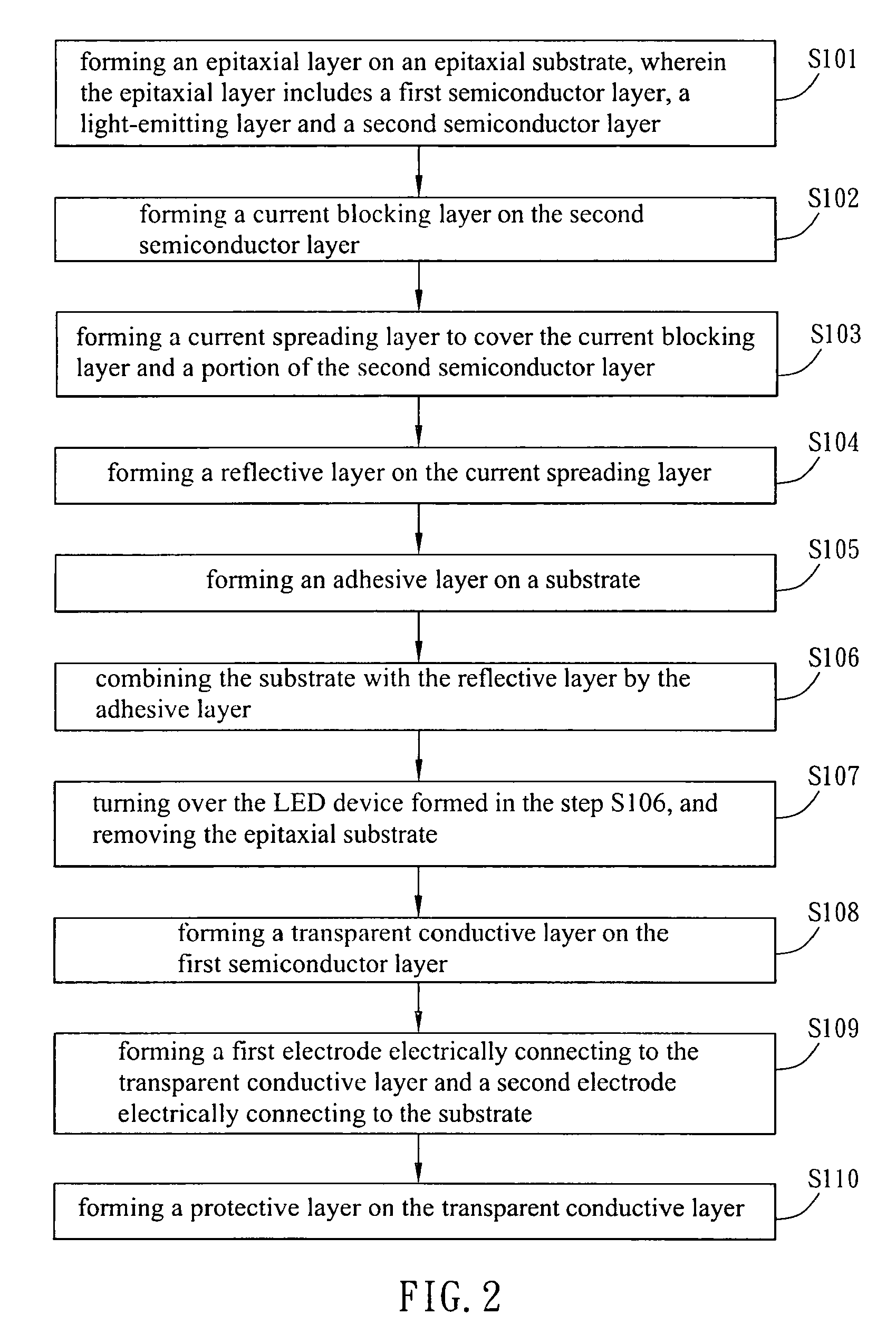
[0024]With reference to FIG. 2, a manufacturing method of a light-emitting diode (LED) device according to a first embodiment of the present invention includes the steps S101 to S110. Illustrations will be made by referring to FIG. 2 in conjunction with FIGS. 3A to 31.

[0025]As shown in FIG. 3A, the step S101 is to form an epitaxial layer 32 on an epitaxial substrate 31. The epitaxial layer 32 includes a first semiconductor layer 321, a light-emitting layer 322 and a second semiconductor layer 323. The first semiconductor layer 321 is formed on the epitaxial substrate 31. Next, the light-emitting layer 322 is formed on the first semiconductor layer 321. Then, the second semiconductor layer 323 is formed on the light-emitting layer 322. The first semiconductor layer 321 and the second semiconductor layer 323 can be, for example but not limited to, an N-type epitaxial layer and a P-type epitaxial layer, respectively. Of course, the first semiconductor layer 321 and the second semicondu...

second embodiment

[0038]With reference to FIG. 4, a manufacturing method of a light-emitting diode (LED) device according to a second embodiment of the present invention includes the steps S201 to S211. Illustrations will be made by referring to FIG. 4 in conjunction with FIGS. 5A to 5J. Herein, the steps S201 to S203 as shown in FIGS. 5A to 5E are similar to the steps S101 to S103 of the first embodiment, so the detailed descriptions will be omitted.

[0039]In step S204, a reflective layer 35 is formed on the current spreading layer 34, and then an insulating thermoconductive layer 40 is formed on the reflective layer 35. In the embodiment, the material of the insulating thermoconductive layer 40 includes nitride, oxide, carbide, aluminum oxide, silicon carbide or any kind of dielectric materials.

[0040]As shown in FIG. 5F, the step S205 is to form an adhesive layer 36 on a substrate 37. Herein, the material of the adhesive layer 36 is capable of adhering at low temperature and can be a non-conductive ...

third embodiment

[0047]With reference to FIG. 6, a manufacturing method of a light-emitting diode (LED) device according to a third embodiment of the present invention includes the steps S301 to S306. Illustrations will be made by referring to FIG. 6 in conjunction with FIGS. 7A to 7E. Herein, the illustration with reference to FIG. 7A is similar to that described in the previous embodiment, so the detailed descriptions will be omitted.

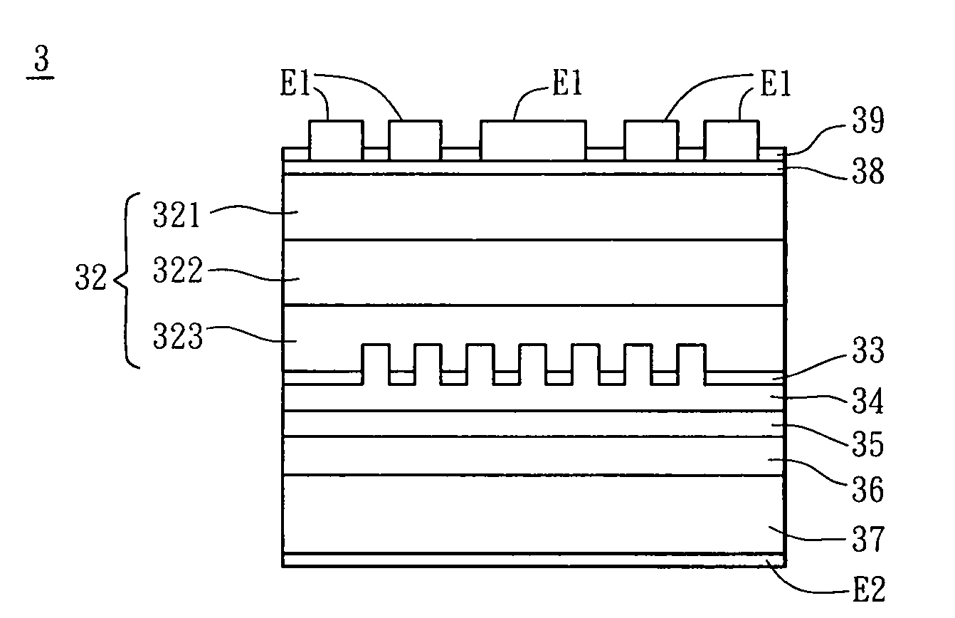
[0048]In the embodiment, the second semiconductor layer 323 is formed on the light-emitting layer 322 and is etched by a thin-film process, a photolithograph process, an etching process, an electron beam writer (E-beam writer) processing, an anodic aluminum oxidizing (AAO) or using micro-nano particles to the first micro-nano structure 323a as shown in FIG. 7B.

[0049]The first micro-nano structure 323a includes at least one nano-ball, nano-column, nano-hole, nano-point, nano-line, a nano-concave-convex structure, periodic hole or non-periodic hole. In the embodiment, t...


PUM


Abstract

A light-emitting diode device includes an epitaxial layer, a current blocking layer and a current spreading layer. The current blocking layer is disposed on one side of the epitaxial layer and contacts with a portion of the epitaxial layer. The current spreading layer is disposed on one side of the epitaxial layer and contacts with at least a portion of the current blocking layer.

Description

CROSS REFERENCE TO RELATED APPLICATIONS[0001]This Non-provisional application claims priority under 35 U.S.C. §119(a) on Patent Application No(s). 096147919 filed in Taiwan, Republic of China on Dec. 14, 2007, the entire contents of which are hereby incorporated by reference.BACKGROUND OF THE INVENTION[0002]1. Field of Invention[0003]The invention relates to a light-emitting diode (LED) device and a manufacturing method thereof.[0004]2. Related Art[0005]A light-emitting diode (LED) device is a lighting device made of semiconductor materials. The LED device has the advantages of small size, low power consumption, no radiation, mercury-free, long lifetime, fast response speed and high reliability. With the continuous progress of the recent technology, the application range thereof covers the information, communication, customer electronics, vehicle, lighting and traffic sign.[0006]With reference to FIG. 1, a conventional LED device 1 includes a substrate 11, an epitaxial layer 12, a b...

Claims


Application Information

Patent Timeline
IPC IPC(8): H01L33/00H01L33/10H01L33/14
CPCH01L33/10H01L33/382H01L33/14
Inventor CHEN, CHAO-MINCHEN, SHIH-PENGSHIUE, CHING-CHUANCHEN, HUANG-KUN
Owner DELTA ELECTRONICS INC
Why Eureka
Try Eureka