Control of hot carrier injection in a metal-oxide semiconductor device

a technology of metal-oxide semiconductor and control device, which is applied in the direction of semiconductor devices, basic electric elements, electrical equipment, etc., can solve the problem of achieve the effect of reducing the degradation of hci in the mos device and not significantly increasing the cost of manufacturing integrated circui

Active Publication Date: 2005-07-21
BELL SEMICON LLC
View PDF2 Cites 44 Cited by
  • Summary
  • Abstract
  • Description
  • Claims
  • Application Information

AI Technical Summary

Benefits of technology

[0008] The present invention meets the above-noted need by providing techniques for beneficially reducing HCI degradation in an MOS device. In accordance with an illustrative embodiment of the invention, an LDMOS is formed having a dummy gate field plate structure which is configured to control an amount of HCI degradation based, at least in part, on an amount of coverage of the dummy gate field plate over a drift region in the device. Moreover, the techniques of the present invention can be used to fabricate an integrated circuit including, for example, an LDMOS device, using conventional MOS compatible process technology. Consequently, the cost of manufacturing the integrated circuit is not significantly increased.

Problems solved by technology

Consequently, the cost of manufacturing the integrated circuit is not significantly increased.

Method used


Image

  • Control of hot carrier injection in a metal-oxide semiconductor device
  • Control of hot carrier injection in a metal-oxide semiconductor device
  • Control of hot carrier injection in a metal-oxide semiconductor device

Examples


Embodiment Construction

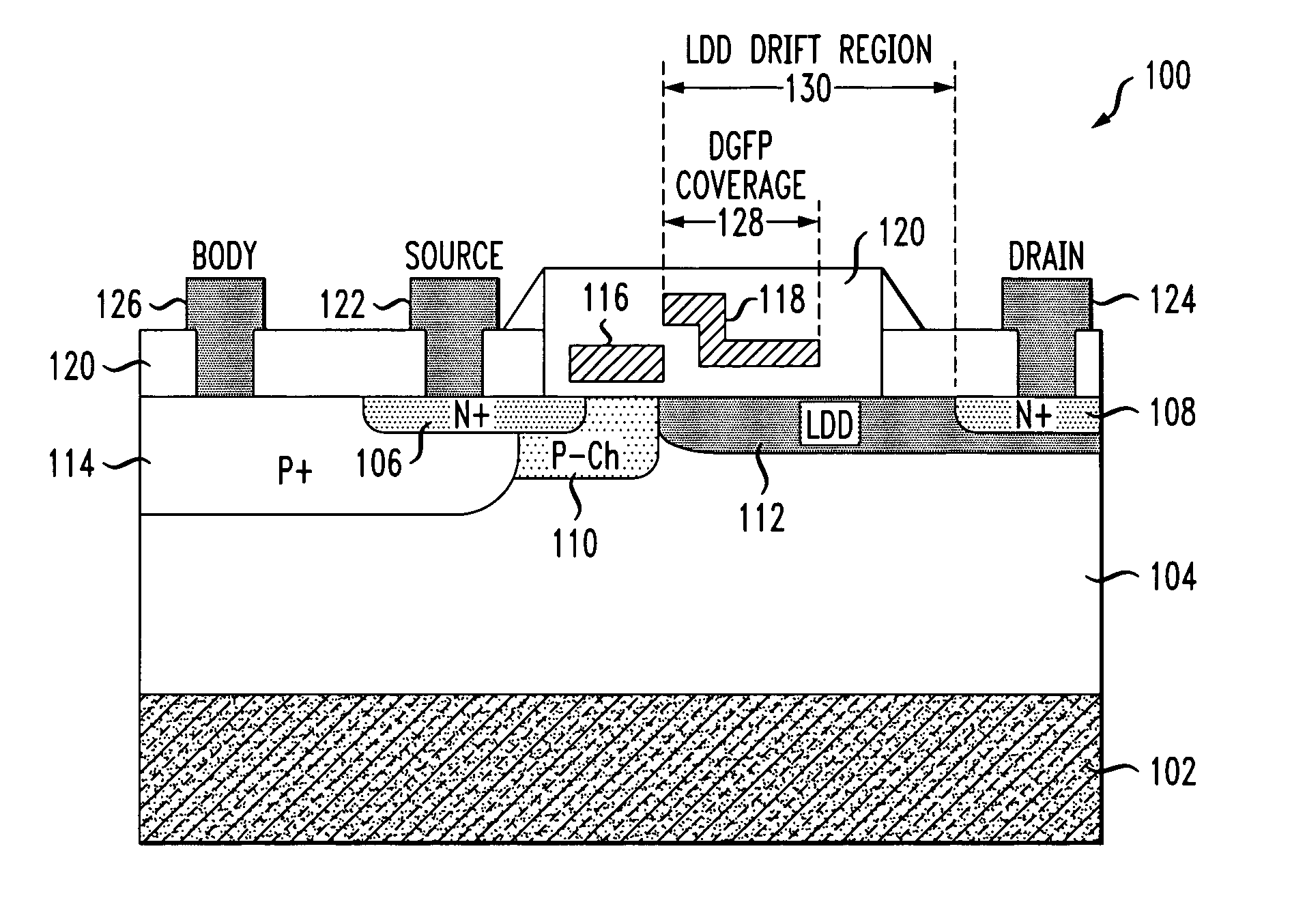
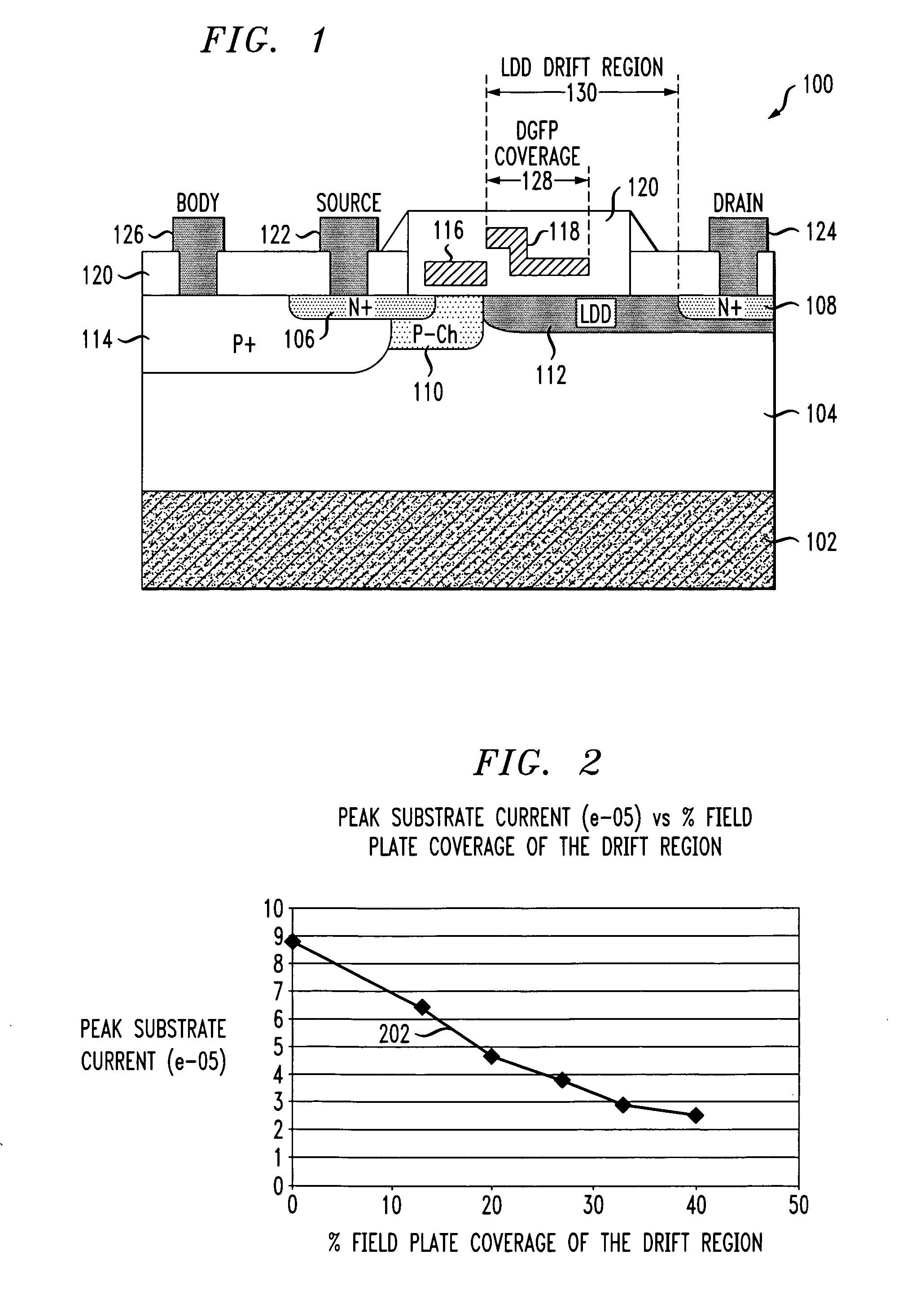
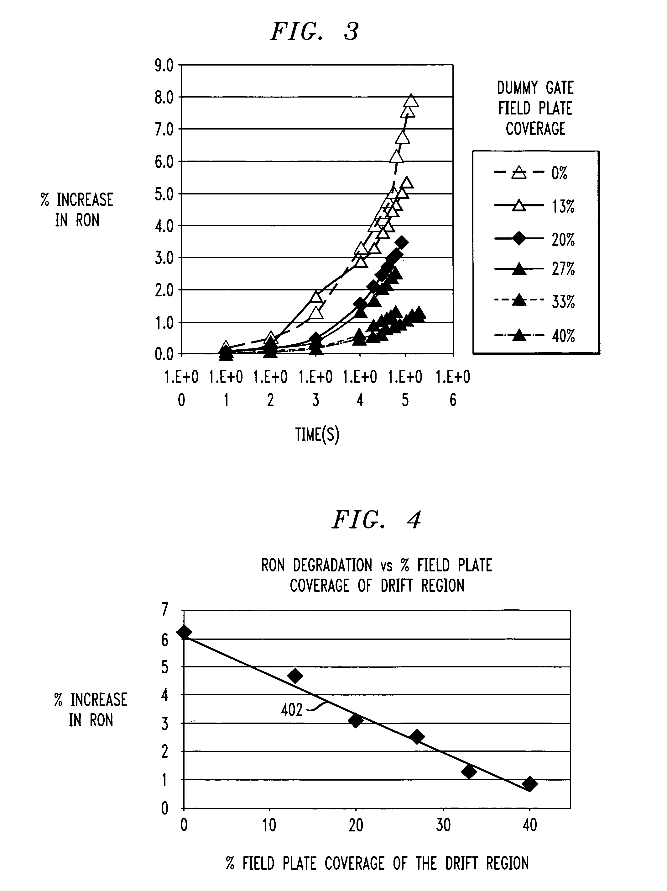
[0013] The present invention will be described herein in the context of an illustrative complementary MOS (CMOS) IC fabrication technology suitable for forming discrete LDMOS transistors, as well as circuits and / or other devices. It should be appreciated, however, that the present invention is not limited to the fabrication of this or any particular circuit or other device. Rather, the invention is more generally applicable to an MOS device comprising a shielding structure which is advantageously configured to control an amount of HCI degradation in the device, without significantly impacting breakdown voltage in the device. Moreover, the shielding structure is fully compatible with a CMOS process technology.

[0014] Although implementations of the present invention are described herein with specific reference to an LDMOS device, it is to be appreciated that the techniques of the present invention are similarly applicable to other devices, as will be understood by those skilled in th...


PUM


Abstract

An MOS device is formed including a semiconductor layer of a first conductivity type, and first and second source/drain regions of a second conductivity type formed in the semiconductor layer proximate an upper surface of the semiconductor layer, the first and second source/drain regions being spaced apart relative to one another. A drift region is formed in the semiconductor layer proximate the upper surface of the semiconductor layer and at least partially between the first and second source/drain regions. An insulating layer is formed on at least a portion of the upper surface of the semiconductor layer and above at least a portion of the drift region. A gate is formed on the insulating layer and at least partially between the first and second source/drain regions. The MOS device further includes a shielding structure formed on the insulating layer above at least a portion of the drift region. The shielding structure is configured such that an amount of hot carrier injection degradation in the MOS device is controlled as a function of an amount of coverage of the shielding structure over an upper surface of the drift region.

Description

CROSS-REFERENCE TO RELATED APPLICATIONS [0001] This application claims the benefit of U.S. Provisional Application Ser. No. 60 / 520,265 filed on Nov. 14, 2003, the disclosure of which is incorporated by reference herein.FIELD OF THE INVENTION [0002] The present invention relates generally to semiconductor devices, and more particularly relates to techniques for controlling hot carrier injection (HCI) degradation in a metal-oxide semiconductor (MOS) device. BACKGROUND OF THE INVENTION [0003] Power MOS devices, including lateral diffused MOS (LDMOS) devices, are employed in a wide variety of applications, such as, for example, power amplifiers in wireless communications systems. HCI degradation can significantly limit the performance of these devices, particularly when operating in a saturation region. As is well known, the HCI phenomenon generally results from heating and subsequent injection of charge carriers into the gate oxide and / or an oxide layer above a drift region of an LDMOS...

Claims


Application Information

Patent Timeline
Patent Type & Authority Applications(United States)
IPC IPC(8): H01L21/336H01L29/40H01L29/41H01L29/76H01L29/78H01L31/113
CPCH01L29/402H01L29/7835H01L29/41
Inventor GAMMEL, PETER L.KIZILYALLI, ISIK C.MASTRAPASQUA, MARCO G.SHIBIB, MUHAMMED AYMANXIE, ZHIJIANXU, SHUMING
Owner BELL SEMICON LLC
Why Eureka
Try Eureka