Dual-gate metal-oxide semiconductor device

a metal-oxide semiconductor and dual-gate technology, applied in the field of semiconductor devices, can solve the problem of not significantly increasing the cost of manufacturing the device, and achieve the effects of improving the high frequency performance of the mos device, reducing the hci degradation of the device, and increasing the hci degradation in the devi

Active Publication Date: 2006-06-01
BELL SEMICON LLC
View PDF2 Cites 46 Cited by
  • Summary
  • Abstract
  • Description
  • Claims
  • Application Information

AI Technical Summary

Benefits of technology

[0006] The present invention meets the above-noted need by providing techniques for beneficially improving high frequency performance of an MOS device, without significantly increasing HCI degradation in the device. In accordance with an illustrative embodiment of the invention, the improved MOS device comprises a dual-gate structure. The dual-gate structure may be formed, for example, by effectively splitting a relatively long gate into two isolated adjacent portions, namely, a first gate configurable for receiving a direct current (DC) bias signal and a second gate configurable for receiving an RF signal. The second gate is substantially short in length so as to achieve a desired low input capacitance, and the first gate is substantially longer than the second gate so as to reduce HCI degradation in the device. By controlling the DC bias signal level applied to the second gate, the device can be selectively turned off while the first gate is connected to an RF input signal. Thus, the techniques of the present invention can be used to provide an internal self-protection mechanism for preventing device failure resulting from an over-power condition. Furthermore, the improved MOS device of the present invention can be fabricated using conventional complementary metal-oxide-semiconductor (CMOS) compatible process technology. Consequently, the cost of manufacturing the device is not significantly increased.

Problems solved by technology

Consequently, the cost of manufacturing the device is not significantly increased.

Method used


Image

  • Dual-gate metal-oxide semiconductor device
  • Dual-gate metal-oxide semiconductor device
  • Dual-gate metal-oxide semiconductor device

Examples


Embodiment Construction

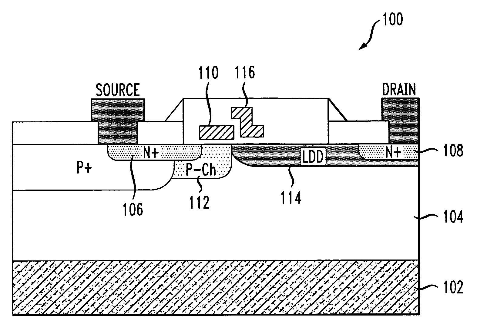
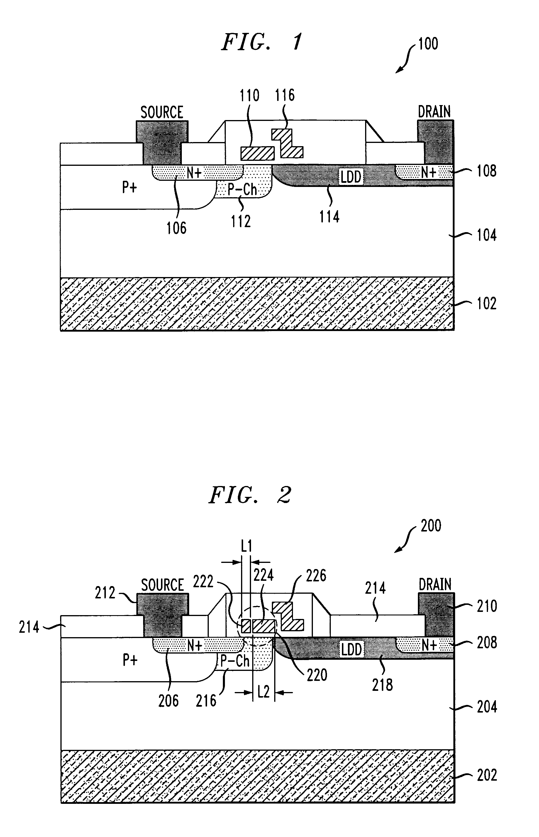
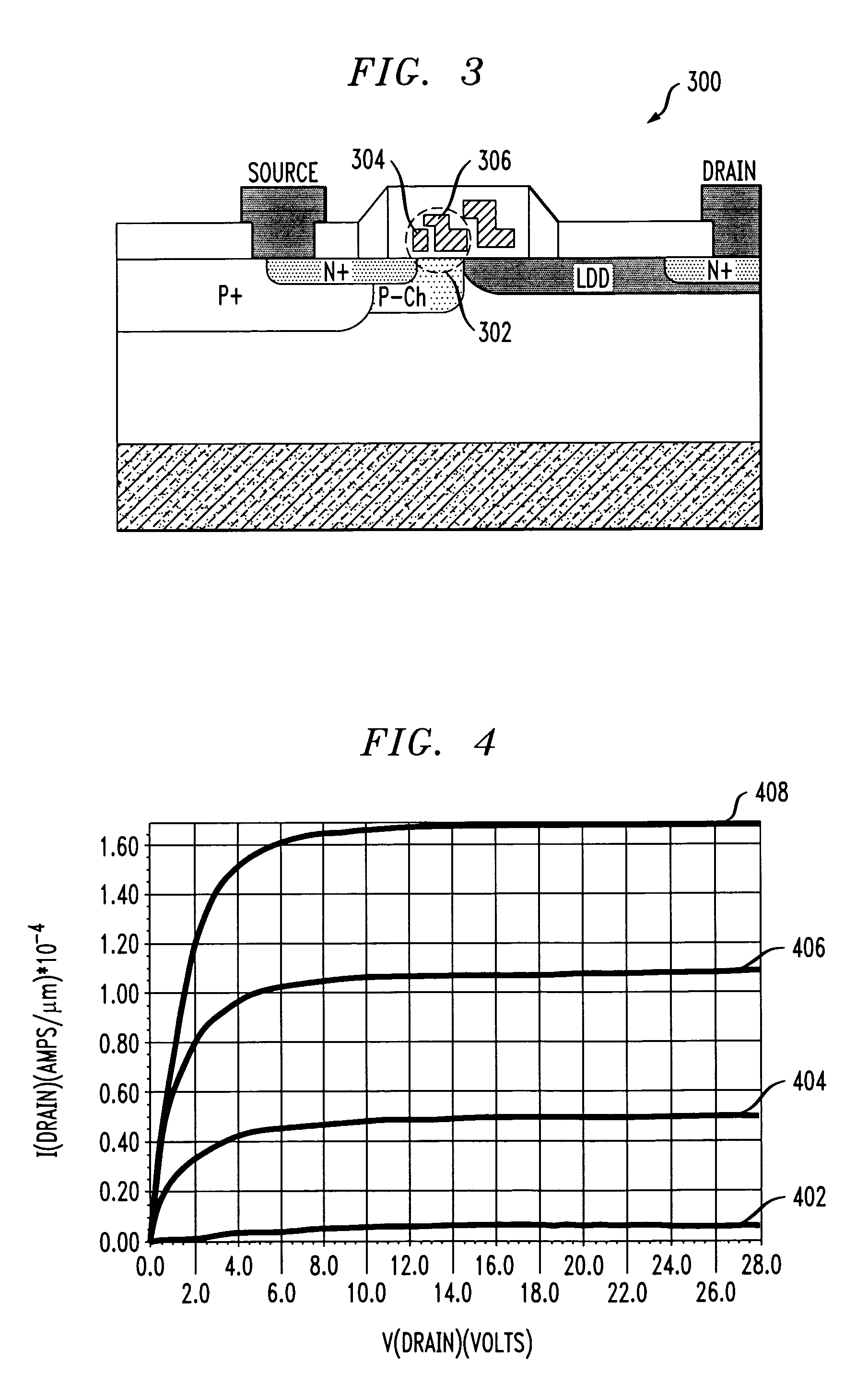
[0015] The present invention will be described herein in the context of an illustrative MOS IC fabrication technology suitable for forming discrete RF LDMOS transistors, as well as other devices and / or circuits. It should be appreciated, however, that the present invention is not limited to the fabrication of this or any particular device or circuit. Rather, the invention is more generally applicable to an MOS device comprising an improved gate arrangement which advantageously enables the MOS device to provide improved high frequency performance and / or reliability, while achieving increased gain and reduced HCI degradation effects. Moreover, the gate arrangement of the present invention can be used to provide an internal self-protection mechanism for protecting the device from failure during an over-power condition to which the device may be subjected.

[0016] Although implementations of the present invention are described herein with specific reference to an LDMOS device, it is to b...


PUM


Abstract

An MOS device includes first and second source/drain regions of a first conductivity type formed in a semiconductor layer of a second conductivity type proximate an upper surface of the semiconductor layer, the first and second source/drain regions being spaced apart relative to one another. A non-uniformly doped channel region of the first conductivity type is formed in the semiconductor layer proximate the upper surface of the semiconductor layer and at least partially between the first and second source/drain regions. An insulating layer is formed on the upper surface of the semiconductor layer. A first gate is formed on the insulating layer at least partially between the first and second source/drain regions and above at least a portion of the channel region, and at least a second gate formed on the insulating layer above at least a portion of the channel region and between the first gate and the second source/drain region. The second gate has a length which is substantially greater than a length of the first gate, the first and second gates being electrically isolated from one another.

Description

FIELD OF THE INVENTION [0001] The present invention relates generally to semiconductor devices, and more particularly relates to techniques for improving the high-frequency performance of a metal-oxide semiconductor (MOS) device. BACKGROUND OF THE INVENTION [0002] Power MOS devices, such as, for example, lateral diffused MOS (LDMOS) devices, are employed in a wide variety of applications, such as, for example, power amplification, switching, etc. In applications where high-frequency operation is desired, such as in a radio frequency (RF) range (e.g., above about 1 gigahertz (GHz)), a conventional LDMOS device generally uses a shorter gate length, in comparison to the gate length of a typical LDMOS device that is not adapted for high frequency applications, in order to improve the RF performance of the device. When operating the device in the RF frequency range, a shorter gate length is generally necessary for achieving a high input impedance. However, reducing the gate length undesi...

Claims


Application Information

Patent Timeline
Patent Type & Authority Applications(United States)
IPC IPC(8): H01L29/06
CPCH01L29/402H01L29/7831H01L29/7835
Inventor SHIBIB, MUHAMMED AYMANXU, SHUMING
Owner BELL SEMICON LLC
Why Eureka
Try Eureka