Semiconductor device and manufacturing method thereof

a semiconductor and film technology, applied in semiconductor devices, capacitors, electrical devices, etc., can solve the problems of capacitive insulation film film quality degradation and inability to obtain sufficient electrical characteristics of capacitors, and achieve the effect of preventing mutual reaction

Inactive Publication Date: 2005-07-28
LAPIS SEMICON CO LTD
View PDF19 Cites 1 Cited by
  • Summary
  • Abstract
  • Description
  • Claims
  • Application Information

AI Technical Summary

Benefits of technology

[0010] The object of the present invention is to provide a more highly reliable semiconductor device, and a method of manufacturing such as device, in which a capacitor using an insulating film made of a metal oxide as a capacitive insulation film has a protective film for sufficiently preventing diffusion of H2, and film quality degradation of the capacitive insulation film due to mutual reaction is prevented.
[0016] According to the present invention having these structures, it is possible to prevent mutual reaction between the protective film and the capacitor material, and as a result it is possible to provide a semiconductor that does not suffer from degradation of capacitor characteristics.

Problems solved by technology

With a capacitor having the protective film of the related art, mutual reaction inside the reducing atmosphere of a step of a manufacturing process after formation of the capacitor is caused by combining materials of a protective film for preventing diffusion of H2 to a capacitive insulation film made from a metal oxide insulation film, an upper electrode and a lower electrode, and this causes degradation in the film quality of the capacitive insulation film.
As a result, with a capacitor having a conventional protective film, there is a problem that it is not possible to obtain sufficient electrical characteristics of the capacitor.

Method used


Image

  • Semiconductor device and manufacturing method thereof
  • Semiconductor device and manufacturing method thereof
  • Semiconductor device and manufacturing method thereof

Examples


first embodiment

[0024] the present invention will be described in the following with reference to the drawings.

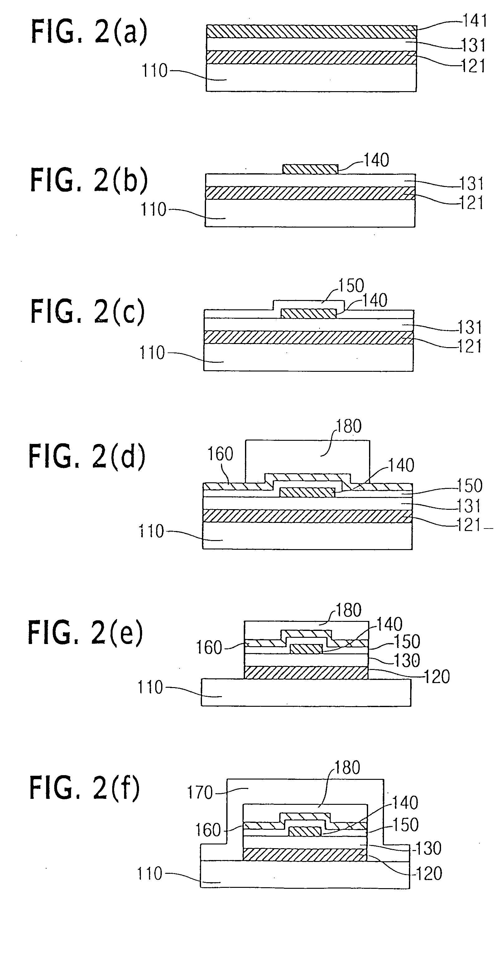
[0025]FIG. 1 and FIG. 2 are drawings showing a first embodiment of the present invention, FIG. 1 being a cross sectional drawing showing a semiconductor device of the first embodiment, and FIG. 2(a)-(f) being cross sectional drawings showing respective processes of a manufacturing method for the semiconductor device of this embodiment.

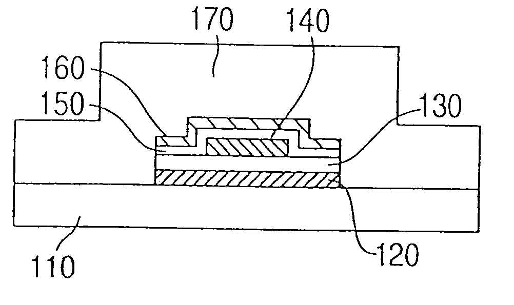
[0026] First of all, a description will be given of the structure of a semiconductor device of this embodiment, using FIG. 1.

[0027] As shown in FIG. 1, a lower electrode 120, a capacitive insulation film 130 and an upper electrode 140 are sequentially deposited on a semiconductor substrate 110 made up of memory cell transistors and peripheral transistors, being semiconductor elements constituting, for example, a semiconductor storage device.

[0028] With the capacitor of the semiconductor of this embodiment, the upper electrode 140 constituting the capacitor...

second embodiment

[0071] Next, the present invention will be described with reference to the drawings.

[0072]FIG. 4 and FIG. 5 are drawings showing a second embodiment of the present invention, FIG. 4 being a cross sectional drawing of a semiconductor device of this embodiment, and FIG. 5(a)-(f) being cross sectional drawings showing respective processes of a manufacturing method for the semiconductor device of this embodiment. In FIG. 4 and FIG. 5, the same reference numerals are used for parts that are the same as in the first embodiment.

[0073] With the semiconductor device of this second embodiment, the difference from the above described first embodiment is that the protective film is provided so as to directly cover the upper surface of the capacitor, namely the upper surface of the upper electrode and the capacitive insulation film, has an element constituting a crystallized core of at least the capacitive insulation film, and is formed from a metal oxide material having a compositional ratio o...


PUM


Abstract

A semiconductor device of the present invention includes capacitors made up of a lower electrode, a capacitive insulation film made from metal oxide material, provided on one surface of a semiconductor substrate. An ozone TEOS film is provided on these capacitors, and a protective film for covering the upper surfaces of the capacitors is then provided on this ozone TEOS film. An interlay insulation film that is thicker than the ozone TEOS film is provided on the protective film for covering the upper surfaces of the capacitors. In this way, the present invention prevents degradation in film quality of the capacitive insulation film due to mutual reaction etc. As a result, it becomes possible to provide a capacitor using an insulating film made of a metal oxide as a capacitive insulation film, having a protective film for sufficiently preventing diffusion of H2, a semiconductor device having high reliability, and a method of manufacturing such a semiconductor device, are provided.

Description

BACK GROUND OF THE INVENTION [0001] The present invention relates to a semiconductor device and manufacturing method thereof, and particularly to effective technology applied to a semiconductor device having capacitive elements using an insulating film made from metallic oxide as a capacitive insulation film and a manufacturing method thereof. [0002] In the related art, DRAMs (Dynamic random access memory) provided with transistors and capacitors are a typical example of a semiconductor storage device. [0003] Capacitors constituting a DRAM are made of an upper electrode and a lower electrode, and a capacitive insulation film provided between these two electrodes. An insulation film made from a silicon compound such as a silicon oxide film or a nitride film is generally used as this capacitive insulation film Also at the present time, the use of high dielectric film or ferroelectric films, having smaller surface area but large capacitance compared to conventional capacitive insulatio...

Claims


Application Information

Patent Timeline
Patent Type & Authority Applications(United States)
IPC IPC(8): H01L21/02
CPCY10S438/957H01L28/55
Inventor IGARASHI, YASUSHI
Owner LAPIS SEMICON CO LTD
Why Eureka
Try Eureka