Semiconductor Device and Method for Fabricating the Same

a technology of semiconductor devices and insulating films, which is applied in the direction of semiconductor devices, semiconductor/solid-state device details, electrical equipment, etc., can solve the problems of insufficient adhesiveness, copper has a poor adhesiveness with an insulating film, and the characteristics of transistors are often degraded, etc., to achieve high reliability, excellent mechanical strength, and low resistance

Active Publication Date: 2008-03-06
PANNOVA SEMIC
View PDF9 Cites 26 Cited by
  • Summary
  • Abstract
  • Description
  • Claims
  • Application Information

AI Technical Summary

Benefits of technology

[0052] With a semiconductor device according to the present invention and a method for fabricating the semiconductor device, a highly reliable semico

Problems solved by technology

In general, copper is easily defused in an insulating film such as a silicon oxide film by heat or electric field and this causes degradation of characteristics of transistors in many cases.
Moreover, copper has a poor adhesiveness with an insulating film.
However, a sufficient adhesiveness can not be achieved by this method.
Furthermore, when a titanium film or a titanium nitride film is used as the second barrier metal film 107 (in the case of FIG. 5(a)) or the third barrier metal film 109 (in the case of FIG. 5(b)), the same problem as that in the above-described case where a tantalum film is used arises.
Therefore, when a copper seed layer is forme

Method used


Image

  • Semiconductor Device and Method for Fabricating the Same
  • Semiconductor Device and Method for Fabricating the Same
  • Semiconductor Device and Method for Fabricating the Same

Examples


first embodiment

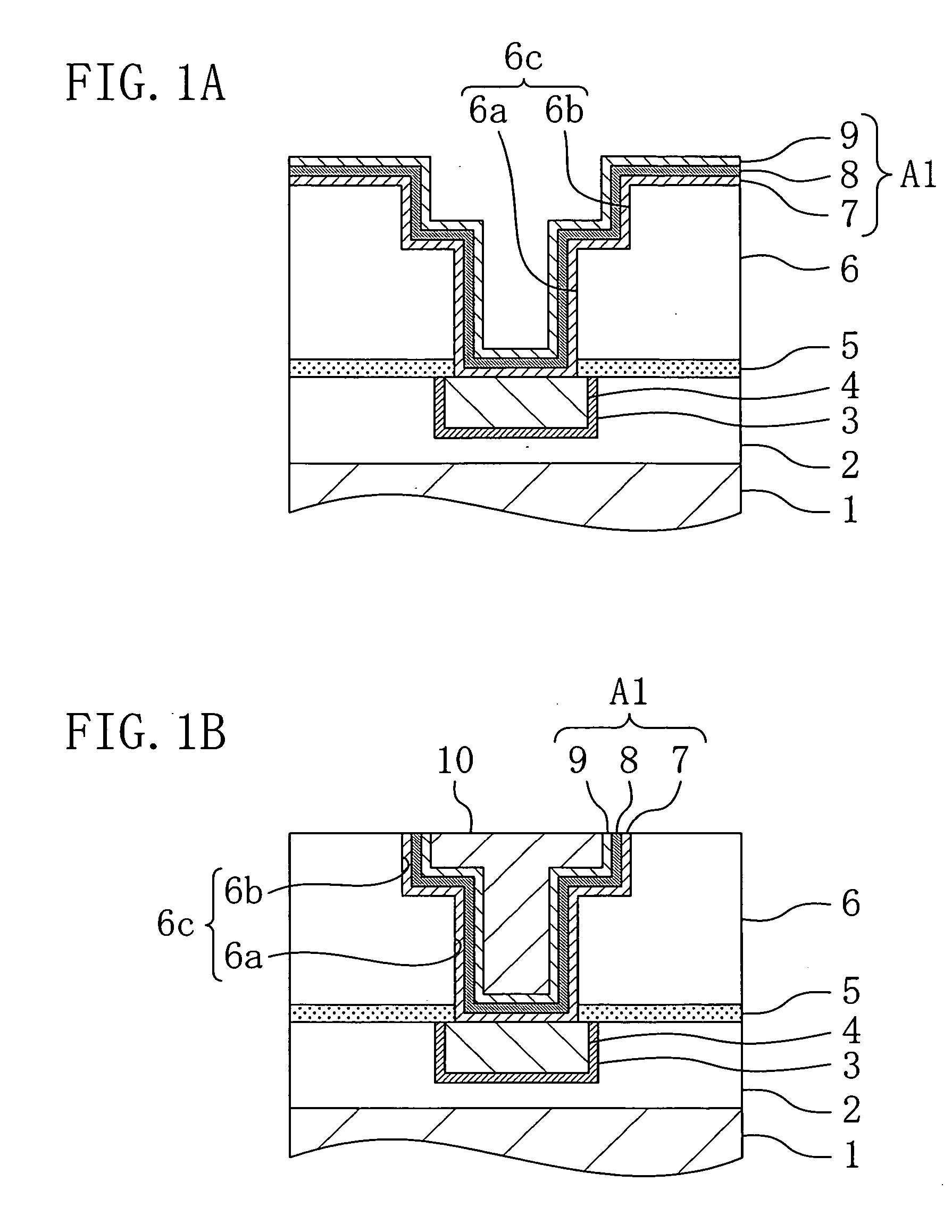
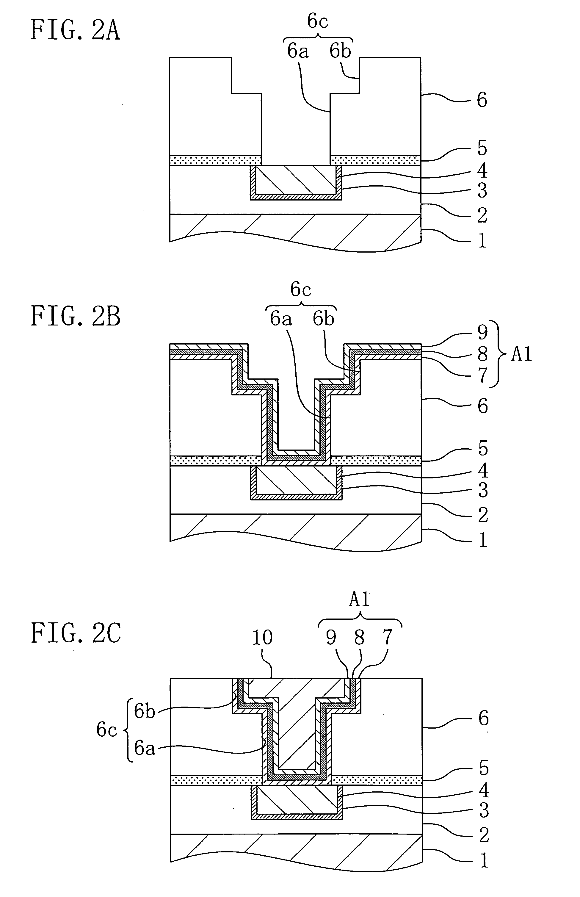
[0085] Hereafter, a semiconductor device according to a first embodiment of the present invention and a method for fabricating the semiconductor device will be described with reference to FIGS. 1(a) and 1(b) and FIGS. 2(a) through 2(c).

[0086] FIGS. 1(a) and 1(b) are cross-sectional view illustrating major part of a structure of a semiconductor device according to a first embodiment of the present invention.

[0087] First, as shown in FIG. 1(a), a first insulating film 2 is formed on a silicon substrate 1 and a first copper interconnect 4 including a first barrier metal film 3 is formed on the first insulating film 2. Note that transistors and the like, which are not shown in FIGS. 1(a) and 1(b), are formed over the silicon substrate 1. A diffusion barrier film 5 for preventing diffusion of copper and a second insulating film 6 are formed in this order over the first insulating film 2 and the first copper interconnect 4. A via hole 6a is formed in the diffusion barrier film 5 and the...

second embodiment

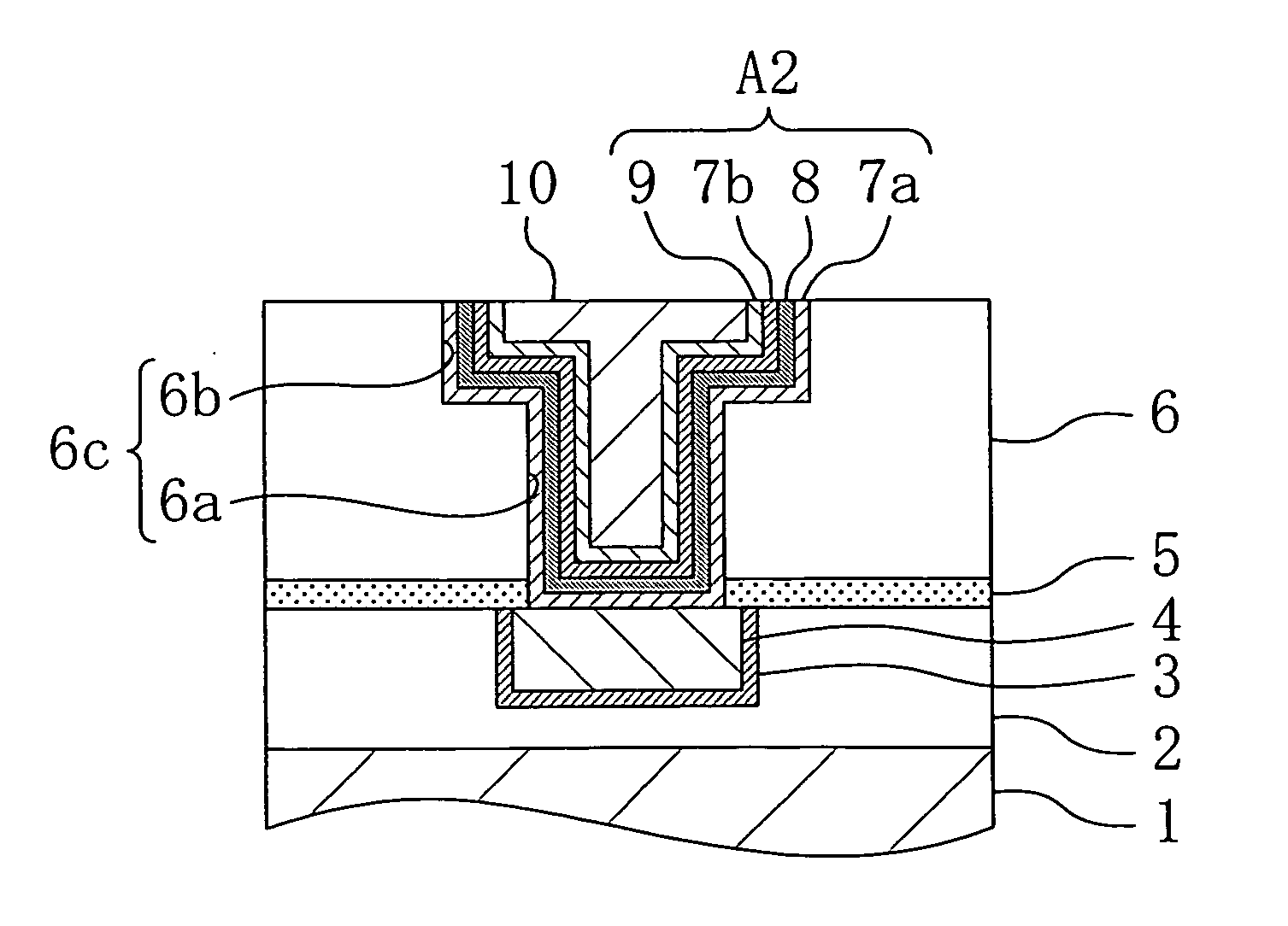
[0122] Hereafter, a semiconductor device according to a second embodiment of the present invention and a method for fabricating the semiconductor device will be described with reference to FIGS. 3(a) and 3(b) and FIGS. 4(a) through 4(c). Note that in the second embodiment, description of each member also shown in the first embodiment is not repeated. Hereafter, description will be made focusing on different points from the first embodiment.

[0123] First, FIGS. 3(a) and 3(b) are cross-sectional views illustrating major part of a structure of a semiconductor device according to the second embodiment of the present invention.

[0124] In FIGS. 3(a) and 3(b), the second embodiment is different from the first embodiment in that a second barrier metal film A2 is formed on wall surfaces of the recess portion 6c and the second barrier metal film A2 includes a first metal oxide film 7a formed on the second insulating film 6, a metal compound film 8 formed on the first metal oxide film 7a, a se...


PUM


Abstract

In a semiconductor device including: an insulating film (6) formed over a substrate (1); a buried metal interconnect (10) formed in the insulating film (6); and a barrier metal film (A1) formed between the insulating film (6) and the metal interconnect (10), the barrier metal film (A1) includes a metal oxide film (7), a metal compound film (8) and a metal film (9) stacked in this order from a side in which the insulating film (6) exists to a side in which the metal interconnect (10) exists. Elastic modulus of the metal compound film (8) is larger than that of the metal oxide film (7).

Description

TECHNICAL FIELD [0001] The present invention relates to a semiconductor device including a copper interconnect and a method for fabricating the semiconductor device, and more particularly relates to a barrier metal film and a method for forming the barrier metal film. BACKGROUND ART [0002] In recent years, as the processing size of semiconductor integrated circuit devices (which will be referred to as “semiconductor devices”) has been reduced, a combination of a copper interconnect and an insulating film having a small dielectric constant, i.e., a so-called low-k film has been used for multilayer interconnects of semiconductor devices. Use of such combination for multilayer interconnects allows reduction in RC delay and in power consumption. Furthermore, to achieve increase in the integration, function and operation speed of semiconductor devices, use of a low-k film having a lower dielectric constant has been under examination. [0003] Copper interconnects are normally formed by dam...

Claims


Application Information

Patent Timeline
IPC IPC(8): H01L23/48H01L21/44
CPCH01L21/76831H01L21/76843H01L21/76846H01L23/53238H01L2924/0002H01L23/53295H01L2924/00H01L21/28
Inventor IKEDA, ATSUSHINAKAGAWA, HIDEOAOI, NOBUO
Owner PANNOVA SEMIC
Why Eureka
Try Eureka