

Semiconductor device and method of fabricating the same
a semiconductor and device technology, applied in the field of semiconductor devices, can solve the problems of high deterioration, inability to prevent deterioration of on currents, and inability to concurrently satisfy the characteristics of the on region and the off region, and achieve the effect of excellent characteristics and highly reliable semiconductors
- Summary
- Abstract
- Description
- Claims
- Application Information
AI Technical Summary
Benefits of technology
Problems solved by technology
Method used
Image

Examples
embodiment mode 1
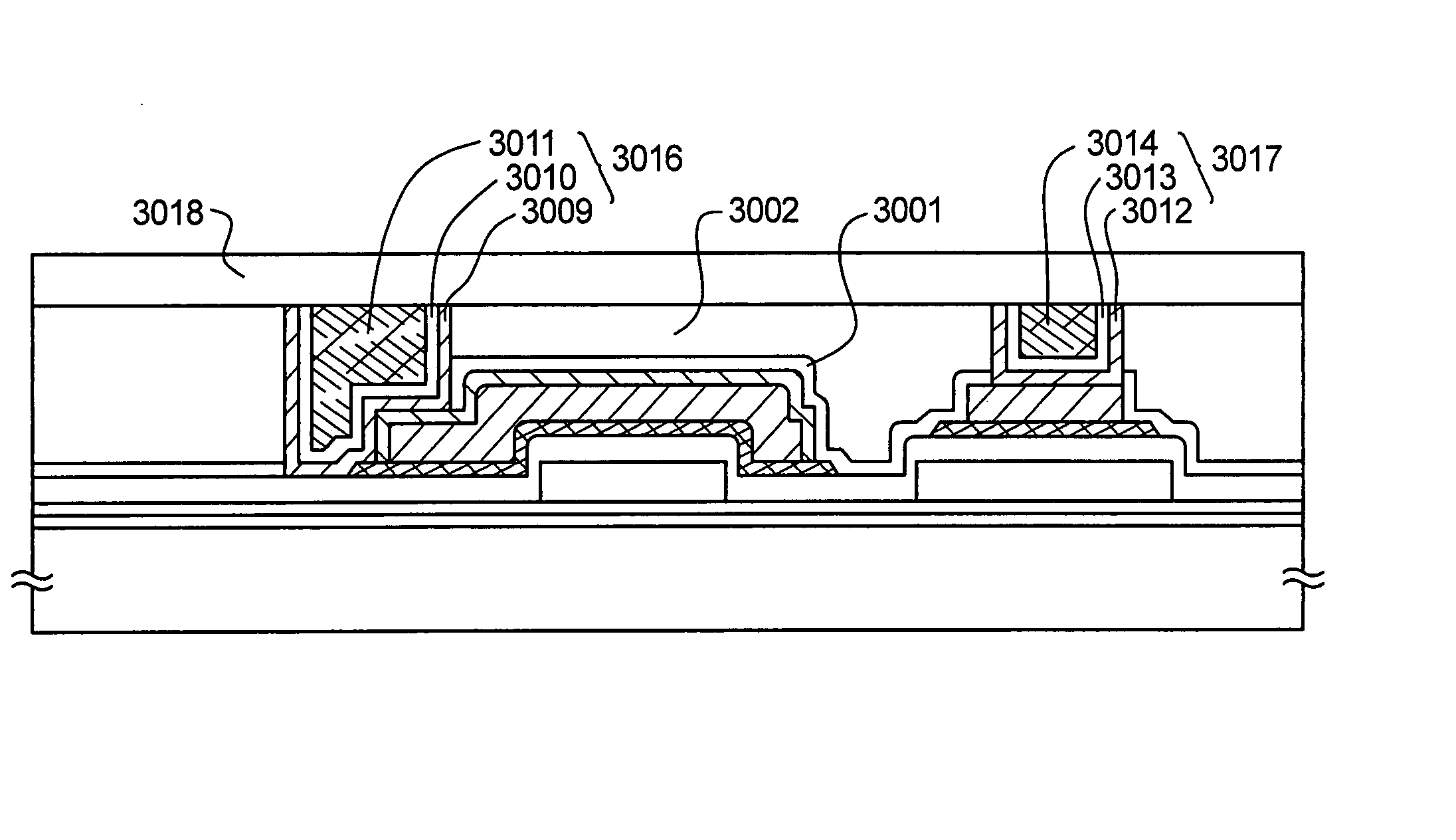
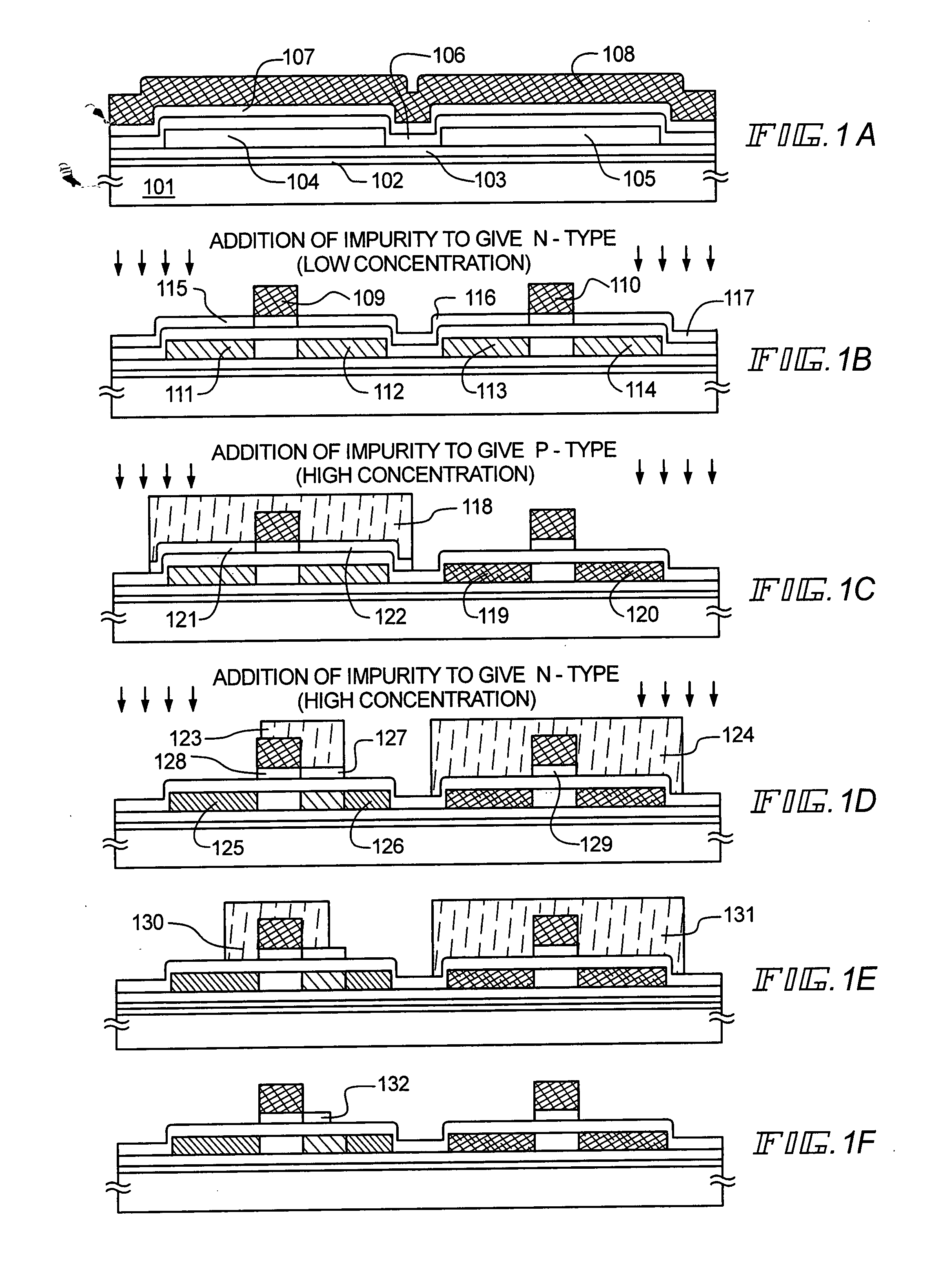
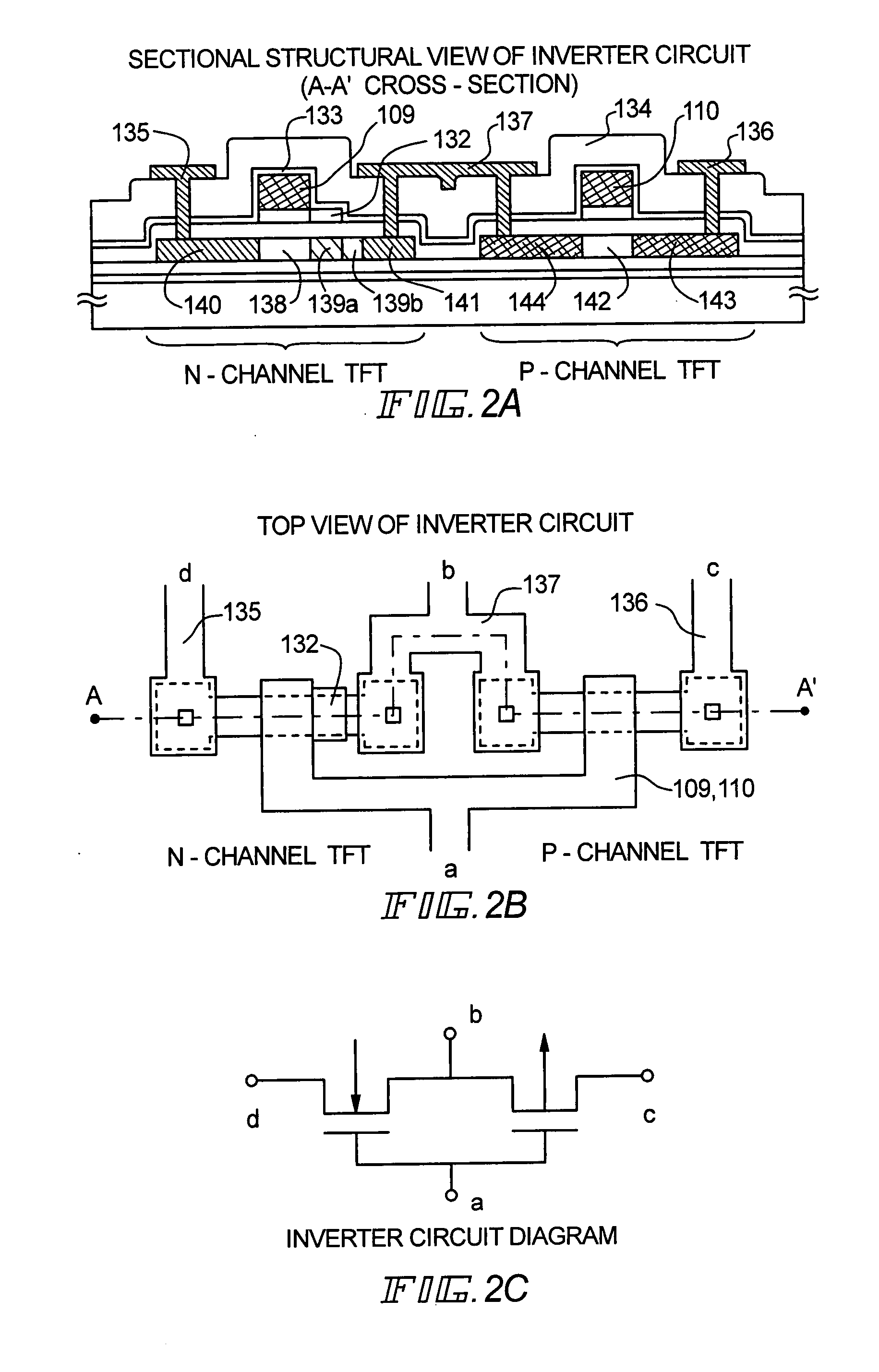
[0163] The mode of carrying out the present invention will be described with reference to FIGS. 1A to 1F and FIGS. 2A to 2C. Here, a description will be made on an example in which an n-channel TFT and a p-channel TFT are fabricated on a substrate at the same time to form an inverter circuit as a basic structure of a CMOS circuit.
[0164] As a substrate 101 having an insulating surface, a glass substrate, a plastic substrate, a ceramic substrate, or the like may be used. Besides, a silicon substrate in which an insulating film such as a silicon oxide film is formed on its surface, or a stainless substrate may be used. A quartz substrate may also be used.
[0165] An under film 102 made of a silicon nitride film and an under film 103 made of a silicon oxide film are formed on a surface of the substrate 101 on which a TFT is to be formed. These under films may be formed by a plasma CVD method or a sputtering method, and are provided in order to prevent an impurity from diffusing from the...
embodiment mode 2
[0194] According to the present invention, as shown in FIGS. 3A and 3B, a second impurity region which becomes an LDD region can be divided into second impurity regions 305a and 306a overlapping with a first layer 302 of a gate electrode, and second impurity regions 305b and 306b not overlapping with the gate electrode. That is, LDD regions overlapping with the gate electrode and LDD, regions not overlapping with the gate electrode are formed. Distinctive formation of the regions can be easily carried out by using a mask of photoresist, and was carried out by a first impurity adding step and a second impurity adding step of forming a first impurity region.
[0195] That is, it is possible to arbitrarily set the lengths X1, X2, Y1 and Y2 of the respective LDD regions shown in FIG. 3A within a range. Here, in view of characteristics including reliability of an n-channel TFT, although the second impurity regions 306a and 306b provided at the side of a first impurity region (drain region)...
embodiment 1
[0203] In this embodiment, a structure of the present invention will be described with reference to FIGS. 4A to 6 and a description will be made on a method of simultaneously fabricating a pixel portion and a CMOS circuit as a basic structure of a driver circuit provided on its periphery.
[0204] In FIGS. 4A to 4C, as a substrate 401, an alkali-free glass substrate typified by, for example, a substrate of 1737 glass made by Corning Inc. was used. An under film 402 was formed on the surface of the substrate 401 on which TFTs were to be formed. As the under film 402, although not shown, a silicon nitride film having a thickness of 25 to 100 nm, here, 50 nm, and a silicon oxide film having a thickness of 50 to 300 nm, here, 150 nm were formed. The under film 402 may be formed using only a silicon nitride film or a silicon nitride oxide film.
[0205] The under film 402 may be formed of one layer of the above material or a laminate structure of not less than, or equal to two layers. In all...
PUM
| Property | Measurement | Unit |
|---|---|---|
| voltage | aaaaa | aaaaa |
| thickness | aaaaa | aaaaa |
| thickness | aaaaa | aaaaa |
Abstract
Description
Claims
Application Information