Semiconductor device and electronic device including the semiconductor device

a semiconductor and electronic device technology, applied in the direction of semiconductor devices, electrical devices, transistors, etc., can solve the problems of deterioration of the electrical characteristics of the transistor, and achieve the effects of high on-state current, high integration, and favorable electrical characteristics

Active Publication Date: 2015-12-17
SEMICON ENERGY LAB CO LTD
View PDF0 Cites 22 Cited by
  • Summary
  • Abstract
  • Description
  • Claims
  • Application Information

AI Technical Summary

Benefits of technology

[0010]An object of one embodiment of the present invention is to provide a semiconductor device with favorable electrical characteristics. Another object is to provide a semiconductor device with high on-state current. Another object is to provide a semiconductor device that is suitable for miniaturization. Another object is to provide a highly integrated semiconductor device. Another object is to provide a semiconductor device with low power consumption. Another object is to provide a highly reliable semiconductor device. Another object is to provide a semiconductor device that can retain data even when power supply is stopped. Another object is to provide a novel semiconductor device.
[0019]In one embodiment of the present invention, any of the following semiconductor devices can be provided: a semiconductor device with favorable electrical characteristics, a semiconductor device that is suitable for miniaturization, a semiconductor device with high on-state current, a highly integrated semiconductor device, a semiconductor device with low power consumption, a highly reliable semiconductor device, a semiconductor device which can retain data even when power supply is stopped, and a novel semiconductor device.

Problems solved by technology

Miniaturization of transistors may cause deterioration of the electrical characteristics of the transistors, such as on-state current, off-state current, threshold voltage, and a subthreshold swing (S value).

Method used


Image

  • Semiconductor device and electronic device including the semiconductor device
  • Semiconductor device and electronic device including the semiconductor device
  • Semiconductor device and electronic device including the semiconductor device

Examples


embodiment 1

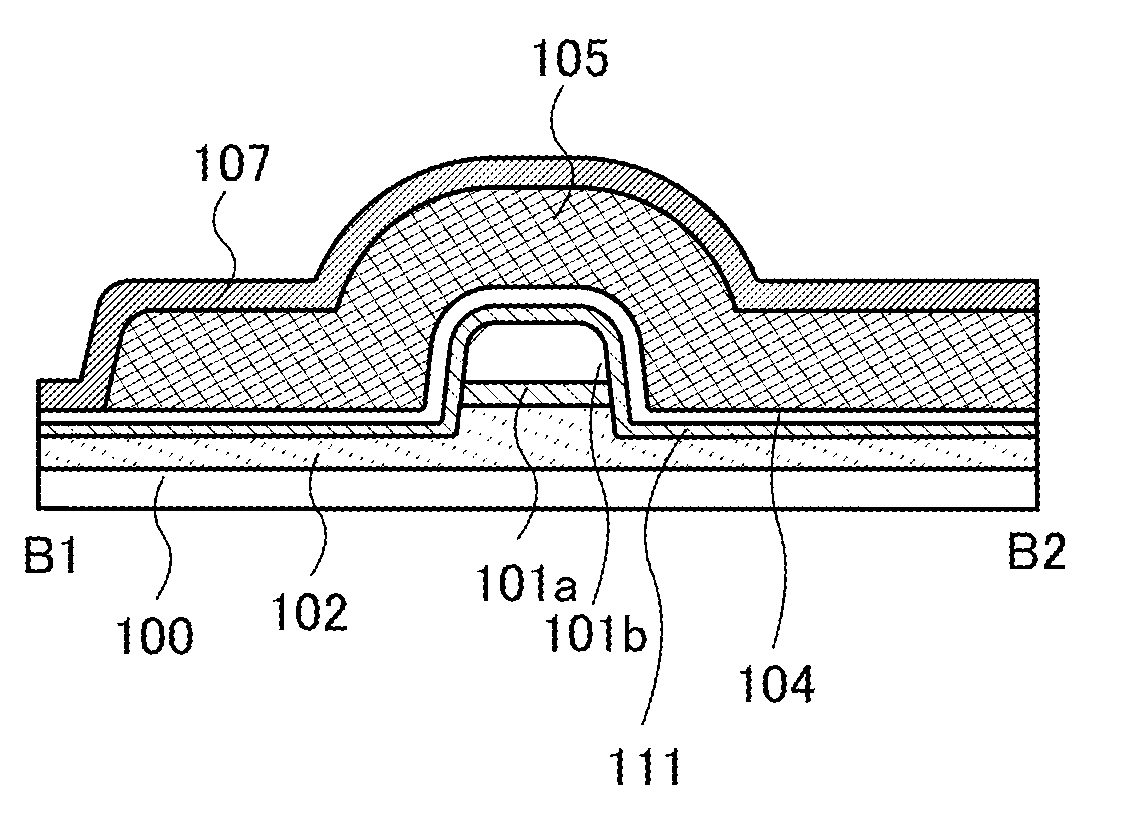
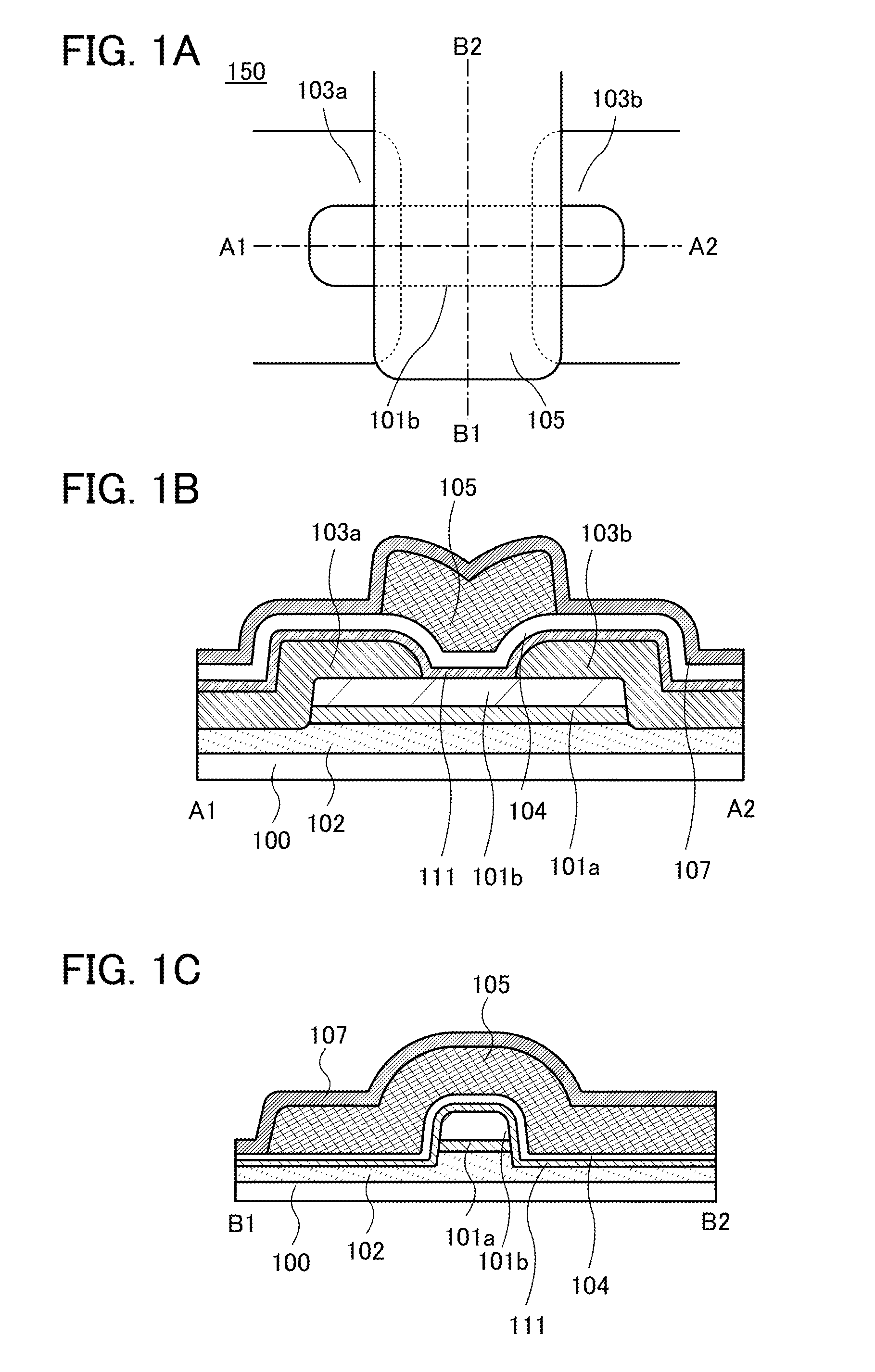
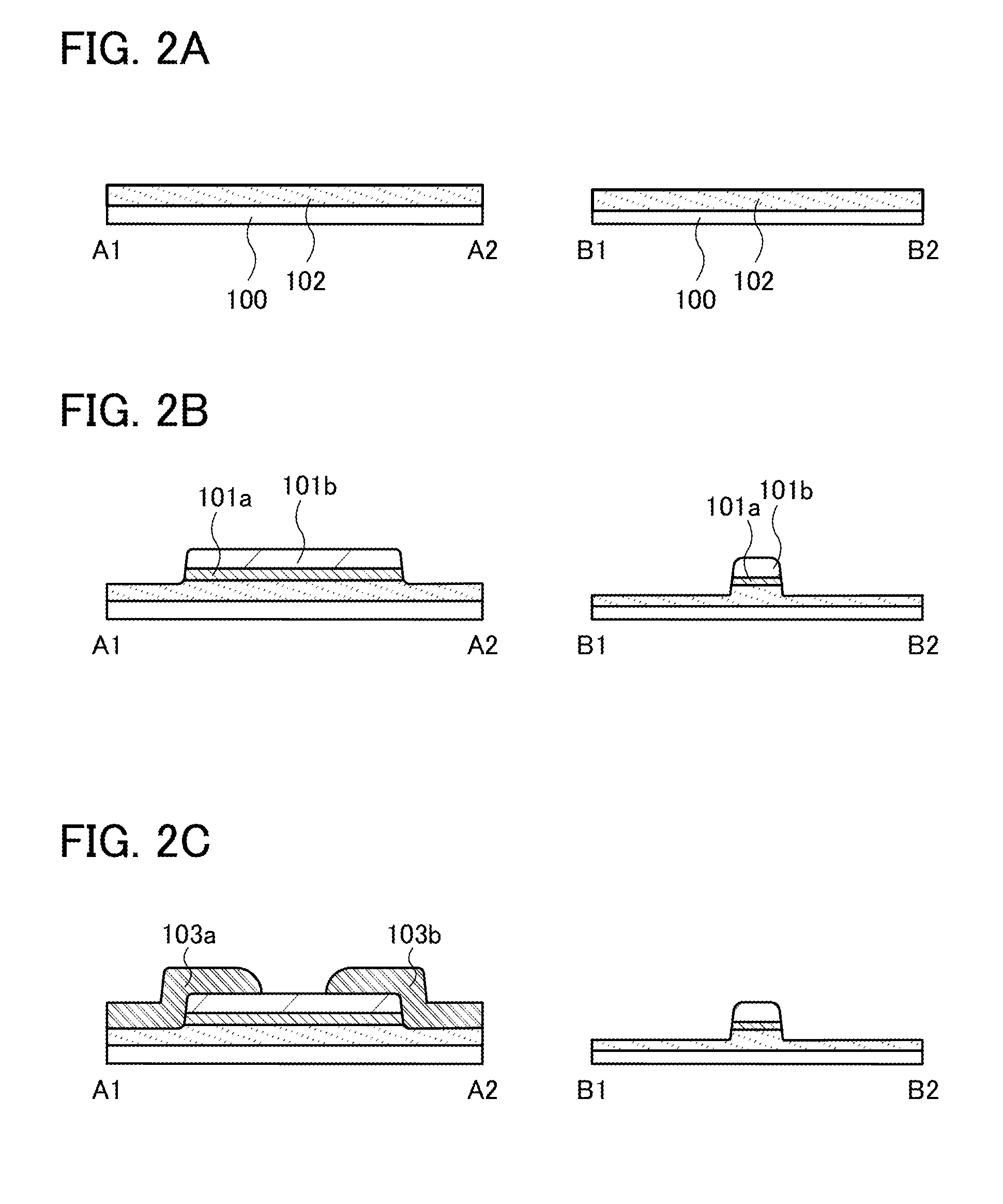
[0058]In this embodiment, a semiconductor device which is one embodiment of the present invention and a manufacturing method thereof will be described with reference to drawings. As an example of a semiconductor device, a transistor will be described.

[0059]In a transistor of one embodiment of the present invention, silicon (including strained silicon), germanium, silicon germanium, silicon carbide, gallium arsenide, aluminum gallium arsenide, indium phosphide, gallium nitride, an organic semiconductor, an oxide semiconductor, or the like can be used for a channel formation region. It is particularly preferable to use an oxide semiconductor having a wider band gap than silicon for the channel formation region.

[0060]For example, the oxide semiconductor preferably contains at least indium (In) or zinc (Zn). Further preferably, the oxide semiconductor contains an oxide represented by an In-M-Zn-based oxide (M represents a metal such as Al, Ti, Ga, Ge, Y, Zr, Sn, La, Ce, Mg, Nd, or Hf).

[...

modification example 1

[0179]Although the transistor 150 described in Embodiment 1 includes the two oxide semiconductor films, the present invention is not limited to this example. There may be a single oxide semiconductor film or three or more oxide semiconductor films. FIGS. 4A to 4C illustrate a case of a single oxide semiconductor film, and FIGS. 5A to 5C illustrate a case of three oxide semiconductor films.

[0180]FIGS. 4A to 4C are a top view and cross-sectional views illustrating a transistor 150a included in a semiconductor device. FIG. 4A is a top view of the transistor 150a. FIG. 4B is a cross-sectional view taken along dashed-dotted line A1-A2 in FIG. 4A. FIG. 4C is a cross-sectional view taken along dashed-dotted line B1-B2 in FIG. 4A. In FIGS. 4A to 4C, some components are enlarged, reduced in size, or omitted for easy understanding.

[0181]FIGS. 5A to 5C are a top view and cross-sectional views illustrating a transistor 150b included in a semiconductor device. FIG. 5A is a top view of the transi...

modification example 2

[0183]FIGS. 6A to 6C are a top view and cross-sectional views illustrating a transistor 150c included in a semiconductor device. FIG. 6A is a top view of the transistor 150c. FIG. 6B is a cross-sectional view taken along dashed-dotted line A1-A2 in FIG. 6A. FIG. 6C is a cross-sectional view taken along dashed-dotted line B1-B2 in FIG. 6A. In FIGS. 6A to 6C, some components are enlarged, reduced in size, or omitted for easy understanding. As in the structure illustrated in FIG. 6B, a side surface of the oxide semiconductor film 101b may be in contact with a layer 113a and a layer 113b.

[0184]The layers 113a and 113b may be formed using a transparent conductor, an oxide semiconductor, a nitride semiconductor, or an oxynitride semiconductor, for example. The layers 113a and 113b may be formed using, for example, a layer containing indium, tin, and oxygen, a layer containing indium and zinc, a layer containing indium, tungsten, and zinc, a layer containing tin and zinc, a layer containi...


PUM


Abstract

A semiconductor device includes a first oxide semiconductor film, a second oxide semiconductor film over the first oxide semiconductor film, a source electrode in contact with the second oxide semiconductor film, a drain electrode in contact with the second oxide semiconductor film, a metal oxide film over the second oxide semiconductor film, the source electrode, and the drain electrode, a gate insulating film over the metal oxide film, and a gate electrode over the gate insulating film. The metal oxide film contains M (M represents Ti, Ga, Y, Zr, La, Ce, Nd, or Hf) and Zn. The metal oxide film includes a portion where x / (x+y) is greater than 0.67 and less than or equal to 0.99 when a target has an atomic ratio of M:Zn=x:y.

Description

TECHNICAL FIELD[0001]One embodiment of the present invention relates to a semiconductor device and a manufacturing method thereof.[0002]Note that one embodiment of the present invention is not limited to the above technical field. The technical field of one embodiment of the invention disclosed in this specification and the like relates to an object, a method, or a manufacturing method. One embodiment of the present invention relates to a process, a machine, manufacture, or a composition of matter. Specifically, examples of the technical field of one embodiment of the present invention disclosed in this specification include a semiconductor device, a display device, a liquid crystal display device, a light-emitting device, a lighting device, a power storage device, a memory device, a method for driving any of them, and a method for manufacturing any of them.[0003]In this specification and the like, a semiconductor device generally means a device that can function by utilizing semico...

Claims


Application Information

Patent Timeline
Patent Type & Authority Applications(United States)
IPC IPC(8): H01L29/786H01L21/477H01L29/10H01L21/02H01L29/66H01L29/04
CPCH01L29/78696H01L29/7869H01L29/66969H01L21/02554H01L29/1033H01L21/02631H01L21/477H01L29/045H01L21/02483H01L21/02488H01L21/02565H01L29/78618H01L21/84H01L29/78621H01L27/1207H01L27/1225H01L27/1248H01L29/41733H01L29/42384
Inventor TSUBUKU, MASASHITAKEUCHI, TOSHIHIKOYAMANE, YASUMASAOOTA, MASASHI
Owner SEMICON ENERGY LAB CO LTD
Why Eureka
Try Eureka