Semiconductor device

a technology of semiconductor devices and semiconductors, applied in semiconductor devices, semiconductor/solid-state device details, electrical apparatus, etc., can solve the problems of heat dissipation ability, device reliability reduction, device thickness reduction and miniaturization, etc., and achieve the effect of efficient dissipation

Active Publication Date: 2013-05-28
FUJI ELECTRIC CO LTD
View PDF24 Cites 23 Cited by
  • Summary
  • Abstract
  • Description
  • Claims
  • Application Information

AI Technical Summary

Benefits of technology

[0013]With the foregoing in view, it is the object of the present invention to provide a semiconductor device in which heat generated from the semiconductor elements carried by the device can be efficiently dissipated and also to provide a method for manufacturing such a semiconductor device.
[0019]According to the disclosed semiconductor device and method for manufacturing, it is possible to realize a highly reliable semiconductor device in which heat generated from the mounted semiconductor element can be efficiently dissipated to the upper and lower main surface sides of the semiconductor device.

Problems solved by technology

However, with some configurations of the conventional semiconductor devices, heat dissipation ability is insufficient and device reliability is reduced, or the increase in heat dissipation ability prevents the devices from being reduced in thickness and miniaturized.

Method used


Image

  • Semiconductor device
  • Semiconductor device
  • Semiconductor device

Examples


first embodiment

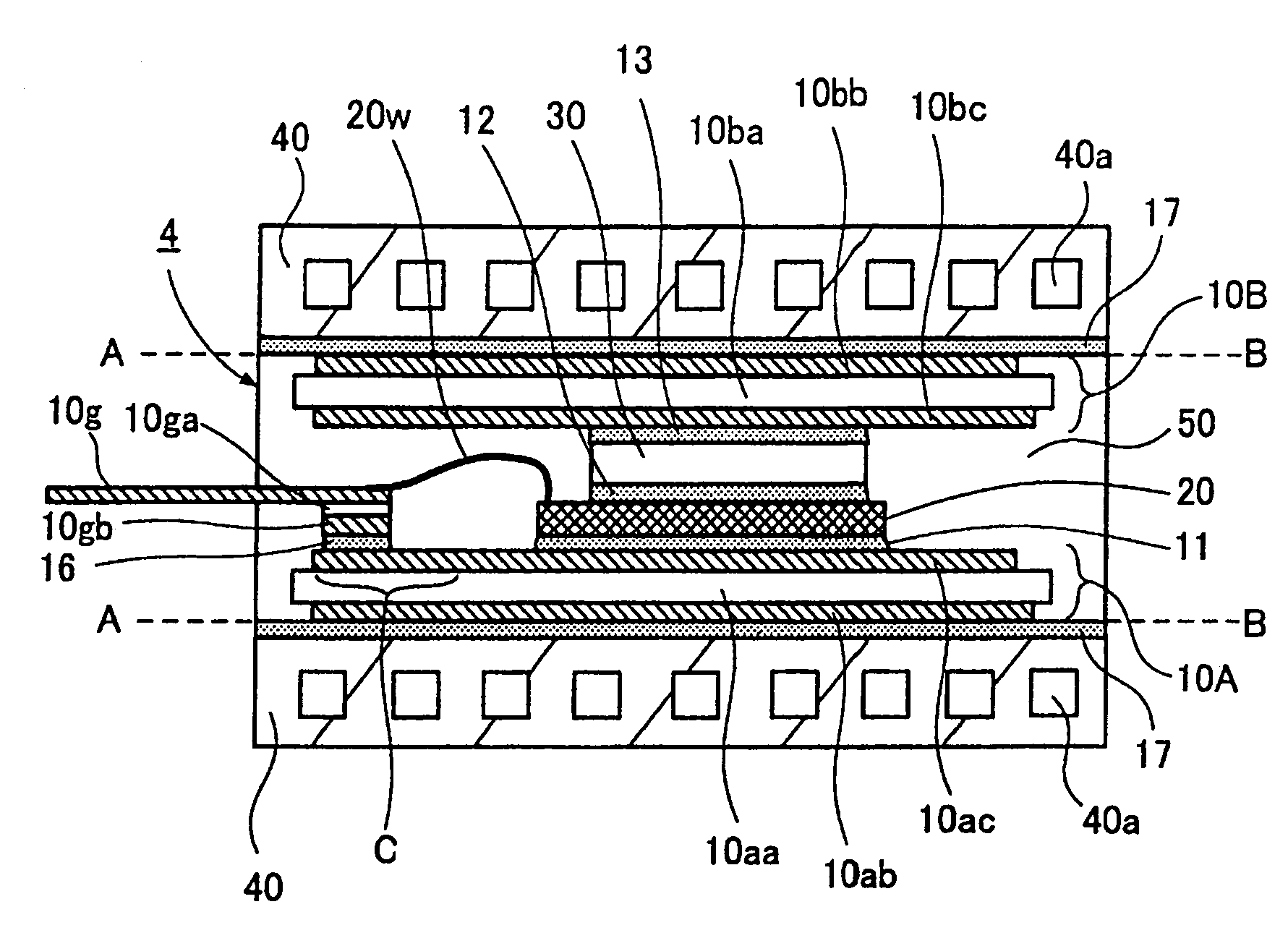
[0059]FIG. 1 is a schematic view of a semiconductor device according to the

[0060]As shown in the figure, in a semiconductor device (semiconductor package) 1, an insulating substrate 10A is taken as a base body, and at least one semiconductor element 20 is mounted on the insulating substrate 10A with a lead-free solder layer 11 of a tin (SN)-silver (Ag) system being interposed therebetween.

[0061]The insulating substrate 10A is provided with an insulating plate 10aa, a metal foil 10ab provided on the lower surface of the insulating plate 10aa, and metal foils 10ac, 10ad provided on the upper surface of the insulating plate 10aa. The metal foil 10ab and the metal foils 10ac, 10ad are selectively and respectively provided on the upper and lower surface of the insulating plate 10aa and separated by the insulating plate 10aa. The metal foil 10ab provided on the lower surface of the insulating plate 10aa includes a portion provided in a region of the insulating plate 10aa that is on the in...

second embodiment

[0152]FIG. 10 is a schematic drawing illustrating a semiconductor device according to the

[0153]As shown in the figure, in a semiconductor device (semiconductor package) 2, an insulating substrate 10A is used as a base body and a metal block body 31 is mounted on the insulating substrate 10A. At least one semiconductor element 20 is mounted on the metal block body 31.

[0154]In this case, the insulating substrate 10A is provided with an insulating plate 10aa, a metal foil 10ab provide on the lower surface of the insulating plate 10aa, and metal foils 10ac, 10ad provided on the upper surface of the insulating plate 10aa. The metal foil 10ab and the metal foils 10ac, 10ad are selectively provided in respective predetermined regions on the upper and lower surfaces of the insulating plate 10aa and are thus separated by the insulating plate 10aa. The metal foils 10ab, 10ac, and 10ad can be formed using, for example, the DCB method.

[0155]Further, the semiconductor element 20 is the so-called...

third embodiment

[0178]FIG. 11 is a schematic drawing illustrating a semiconductor device according to the

[0179]As shown in the figure, in a semiconductor device (semiconductor package) 3, a metal plate (die pad) 33A is used as a base body and at least one semiconductor element 20 is mounted on the metal plate 33A.

[0180]In this case, the semiconductor element 20 is the so-called power semiconductor element and, for example, corresponds to a RC-IGBT element. In addition to the RC-IGBT element, for example, a usual IGBT element, a power MOSFET, and a FWD element can be disposed as the semiconductor element 20.

[0181]In the semiconductor device 3, one main electrode (for example, a collector electrode) of the semiconductor element 20 is joined via a solder layer 11 to the metal plate 33A. A metal plate 30 that functions as a heat spreader or a lead frame is joined via a lead-free solder layer 12 to the other main electrode (for example, an emitter electrode), which is provided oh the main surface on the...


PUM


Abstract

The object of the present invention is to efficiently dissipate heat from the upper and lower main surfaces of a semiconductor device carrying a semiconductor element. A semiconductor device (1) is provided with an insulating substrate (10A), an insulating substrate (10B) provided so as to face the insulating substrate (10A), and a semiconductor element (20) disposed between the insulating substrate (10A) and the insulating substrate (10B) and having a collector electrode and an emitter electrode provided on the side opposite to that of the collector electrode. The collector electrode is electrically connected to a metal foil (10ac) provided on the insulating substrate (10A), and the emitter electrode is electrically connected to the metal foil (10bc) provided on the insulating substrate (10B). As a result, heat generated by the semiconductor element (20) is efficiently dissipated from the upper and lower main surfaces of the semiconductor device (1).

Description

TECHNICAL FIELD[0001]The present invention relates to a semiconductor device carrying a power semiconductor element.BACKGROUND ART[0002]In inverter devices, uninterrupted power supply devices, machine tools, and industrial robots, semiconductor devices (semiconductor packages), which are independent from the main device and carries a power semiconductor elements, are used.[0003]For example, FIG. 16 is a principal view of a semiconductor deviance carrying a power semiconductor element.[0004]As shown in the figure, in a semiconductor device 100, a parallel connection circuit is provided between a metal bar 130a and a metal bar 130b by bringing main electrodes of an IGBT (Insulated Gate Bipolar Transistor) element 110Na and electrodes of a diode 110Nb into contact respectively with the bars, a parallel connection circuit is provided between the metal bar 130b and a metal bar 130c by bringing main electrodes of an IGBT element 110Pa and electrodes of a diode 110Pb into contact respectiv...

Claims


Application Information

Patent Timeline
Patent Type & Authority Patents(United States)
IPC IPC(8): H01L23/34
CPCH01L23/3735H01L23/4334H01L23/473H01L23/49537H01L23/49562H01L23/49575H01L24/29H01L24/32H01L24/33H01L24/40H01L24/73H01L24/83H01L25/072H01L25/117H01L24/80H01L21/4882H01L23/3107H01L24/45H01L24/48H01L2224/29111H01L2224/32225H01L2224/45124H01L2224/45144H01L2224/48091H01L2224/48227H01L2224/48247H01L2224/49171H01L2224/73215H01L2224/73265H01L2224/83801H01L2924/01002H01L2924/01004H01L2924/01005H01L2924/01013H01L2924/01014H01L2924/01029H01L2924/01047H01L2924/0105H01L2924/01051H01L2924/01074H01L2924/01079H01L2924/01082H01L2924/13055H01L2924/13091H01L24/49H01L2224/29H01L2224/2919H01L2224/29298H01L2924/01006H01L2924/01019H01L2924/01033H01L2924/014H01L2924/0665H01L2924/0132H01L2924/1579H01L2924/00013H01L2224/73221H01L2924/12041H01L2924/1306H01L2924/1305H01L2924/00014H01L2924/00H01L2924/00012H01L2224/29099H01L2224/29199H01L2224/29299H01L2224/2929H01L2924/00011H01L2224/40137H01L2924/12042H01L2924/181H01L2224/05554H01L2224/371H01L2224/84801H01L24/37H01L2224/06181H01L24/84H01L2224/2612H01L23/49541H01L23/051H01L25/50H01L24/85H01L2224/83205
Inventor IKEDA, YOSHINARISOYANO, SHINMOROZUMI, AKIRASUZUKI, KENJITAKAHASHI, YOSHIKAZU
Owner FUJI ELECTRIC CO LTD
Why Eureka
Try Eureka