Thermally enhanced semiconductor package

a technology of semiconductor packages and heat dissipation efficiency, applied in semiconductor devices, semiconductor/solid-state device details, electrical apparatus, etc., can solve the problems of inability to accurately correspond to the position of the bond pads, the chip scale package is defective, and the bond pads underneath the first dielectric layer cannot be easily and precisely recognized by lasers, so as to improve the heat dissipation efficiency of the package, improve the production yield of the semiconductor package, and effectively dissipate the heat produced

Inactive Publication Date: 2006-03-28
SILICONWARE PRECISION IND CO LTD
View PDF6 Cites 76 Cited by
  • Summary
  • Abstract
  • Description
  • Claims
  • Application Information

AI Technical Summary

Benefits of technology

[0011]The above semiconductor package utilizes a beat sink directly adhered to the chip, and the heat sink is exposed to outside of the encapsulation body encapsulating the chip and has a surface area equal to that of the package, which can thereby effectively dissipate heat produced from the chip and improve heat dissipating efficiency of the package. Moreover, a plurality of conductive bumps are directly formed on bond pads of the chip, with their ends exposed to outside of the encapsulation body, so as to allow the positions of the bond pads to be easily recognized and allow the conductive traces formed on the encapsulation body to be well electrically connected to the bond pads through the conductive bumps, thereby improving production yield of the semiconductor package. Therefore, the above semiconductor package according to the invention is advantageous over the prior art (FIGS. 5 and 6) in which bond pads of the chip cannot be precisely recognized and completely exposed by vias formed through the dielectric layer (namely, the first dielectric layer applied over the chip) in the use of a laser drilling technique and the incompletely-exposed bond pads degrade their electrical connection with conductive traces subsequently formed on the first dielectric layer.

Problems solved by technology

This chip scale package, however, is defective of not able to provide more surface area, which is limited in accordance with the chip size, for accommodating more solder balls required for the external electrical connection.
However, a significant drawback incurred by the above chip scale package and the encapsulated package structure is that when a laser drilling technique is employed to form vias through the first dielectric layer for exposing the bond pads on the chip, the bond pads underneath the first dielectric layer cannot be easily and precisely recognized by laser in position, making the fabricated vias not able to accurately correspond to the positions of the bond pads.
As a result, the bond pads on the chip cannot be completely exposed, and the incompletely-exposed bond pads would degrade their electrical connection with the first conductive traces formed on the first dielectric layer, thereby damaging production yield of the fabricated packages.
Moreover, as shown in FIG. 6, the chip is entirely encapsulated by the encapsulation body, making heat produced from the chip not able to be effectively dissipated, which may damage the chip by overheat.

Method used


Image

  • Thermally enhanced semiconductor package
  • Thermally enhanced semiconductor package
  • Thermally enhanced semiconductor package

Examples


first preferred embodiment

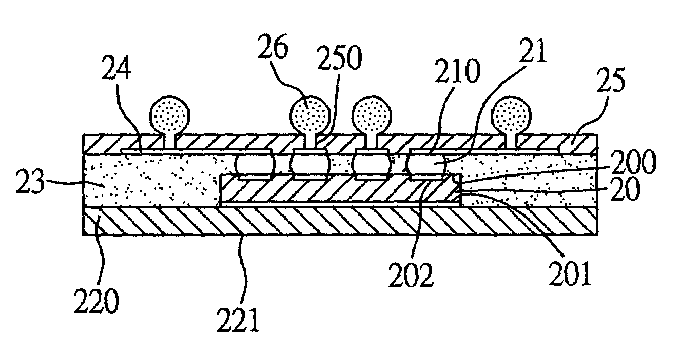
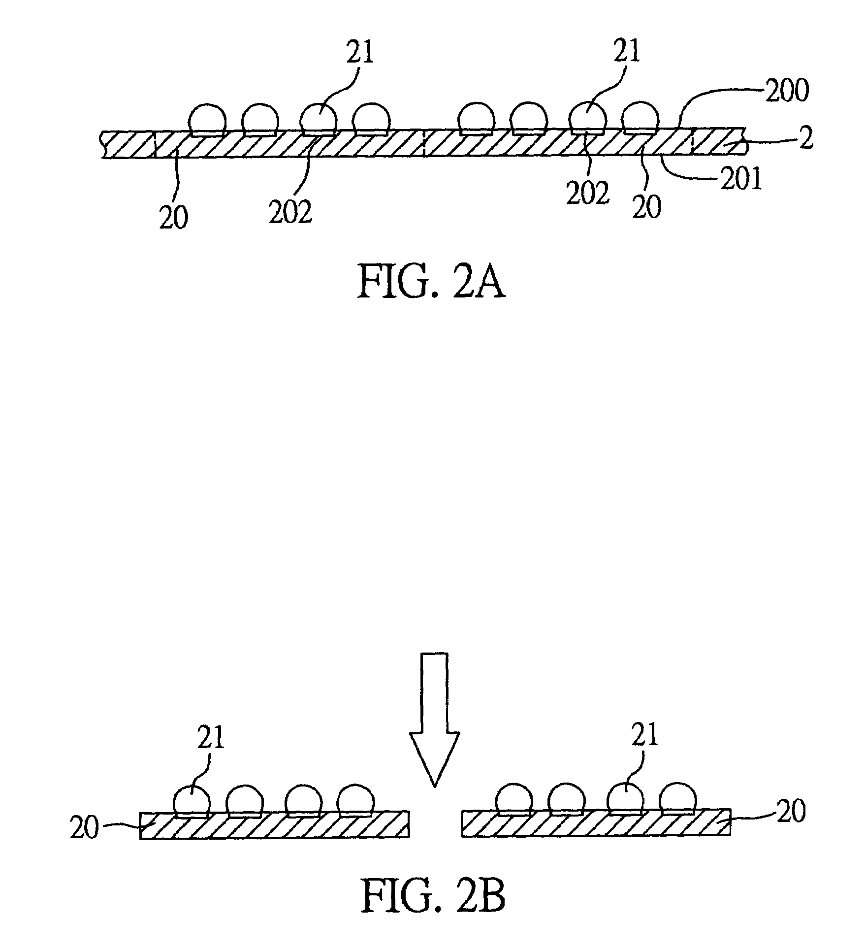
[0020]As shown in FIG. 1, the thermally enhanced semiconductor package according to the first preferred embodiment of the invention comprises: at least one chip 20 having an active surface 200 and an opposite inactive surface 201, the active surface 200 formed with a plurality of bond pads 202 thereon; a conductive bump 21 formed on each of the bond pads 202 of the chip 20; a heat sink 220 attached to the inactive surface 201 of the chip 20 and having a surface area larger than that of the chip 20; an encapsulation body 23 for encapsulating the heat sink 220, chip 20 and conductive bumps 21, wherein a bottom 221 of the heat sink 220 and ends 210 of the conductive bumps 21 are exposed to outside of the encapsulation body 23; a plurality of conductive traces 24 formed on the encapsulation body 23 and electrically connected to the exposed ends 210 of the conductive bumps 21; a solder mask layer 25 applied over the conductive traces 24 and formed with a plurality of openings 250 for exp...

second preferred embodiment

[0031]FIG. 3 illustrates a semiconductor package according to the second preferred embodiment of the invention. As shown in FIG. 3, this semiconductor package is structurally similar to that of the first embodiment, with the difference in that after the conductive traces 24 (hereinafter referred to as “first conductive traces”) are formed on the encapsulation body 23, a dielectric layer 28 is applied over the first conductive traces 24, and a laser drilling technique is employed to form a plurality of vias 280 through the dielectric layer 28 for exposing predetermined portions of the first conductive traces 24. Then, a plurality of second conductive traces 29 are formed on the dielectric layer 28, and each of the second conductive traces 29 is electrically connected to at least one of the exposed portions of the first conductive traces 24.

[0032]Thereafter, the solder mask layer 25 is applied over the second conductive traces 29 and formed with a plurality of openings 250 for exposin...

third preferred embodiment

[0034]FIG. 4 illustrates a semiconductor package according to the third preferred embodiment of the invention. As shown in FIG. 4, this semiconductor package is structurally similar to that of the first embodiment, with the difference in that the surface 223 for attaching the chip 20 of the heat sink 220 is formed with a plurality of recessed portions 222 to allow the resin material forming the encapsulation body 23 and the adhesive 27 adhering the chip 20 and heat sink 220 to fill into the recessed portions 222, so as to enhance adhesion between the surface 223 of the heat sink 220 and the encapsulation body 23 and adhesion between the surface 223 and the chip 20. Alternatively, the surface 223 of the heat sink 220 can be roughened (not shown) to also make the heat sink 220 more strongly adhered to the encapsulation body 23 and the chip 20.


PUM


Abstract

A thermally enhanced semiconductor package and a fabrication method thereof are provided. A plurality of conductive bumps are formed on bond pads on an active surface of a chip. A heat sink is attached to an inactive surface of the chip and has a surface area larger than that of the chip. An encapsulation body encapsulates the heat sink, chip and conductive bumps, while exposing a bottom or surfaces, not for attaching the chip, of the heat sink and ends of the conductive bumps outside. A plurality of conductive traces are formed on the encapsulation body and electrically connected to the ends of the conductive bumps. A solder mask layer is applied over the conductive traces and formed with a plurality of openings for exposing predetermined portions of the conductive traces. A solder ball is implanted on each exposed portion of the conductive traces.

Description

FIELD OF THE INVENTION[0001]The present invention relates to semiconductor packages and fabrication methods thereof, and more particularly, to a thermally enhanced semiconductor package and a method for fabricating the semiconductor package.BACKGROUND OF THE INVENTION[0002]A semiconductor package is a structure used to accommodate at least one integrated circuit component such as semiconductor chip and preferably made compact in size. In correspondence with this goal, there is a type of small scale semiconductor package, named chip scale package (CSP), which has a size substantially equal to or slightly larger than that of the chip incorporated therein.[0003]U.S. Pat. No. 6,287,893 discloses a chip scale package which forms a plurality of build-up layers directly on a semiconductor chip without using a chip carrier such as substrate or lead frame for accommodating the chip. As shown in FIG. 5, the plurality of build-up layers formed on an active surface 100 of the chip 10 include: a...

Claims


Application Information

Patent Timeline
Patent Type & Authority Patents(United States)
IPC IPC(8): H01L23/48H01L23/52H01L29/40H01L23/31H01L23/36H01L23/433H01L23/538
CPCH01L23/3128H01L23/36H01L23/4334H01L23/5389H01L24/18H01L24/97H01L2224/83385H01L2224/92244H01L2224/73267H01L2224/32245H01L2924/01033H01L2224/04105H01L2224/20H01L2224/211H01L2224/92224H01L2224/97H01L2924/01013H01L2924/01029H01L2924/01079H01L2924/01082H01L2924/14H01L2924/15311H01L2224/82H01L2224/83H01L24/19H01L2224/12105H01L2924/12042H01L2924/15159H01L2924/00
Inventor HUANG, CHIEN-PINGHSIAO, CHENG-HSU
Owner SILICONWARE PRECISION IND CO LTD
Why Eureka
Try Eureka