

Semiconductor device utilizing dummy features to form uniform sidewall structures
a technology of sidewall structure and semiconductor, applied in the field of semiconductor devices, can solve the problems of degrading the reliability of the resultant semiconductor device, and achieve the effect of high-reliability semiconductor
- Summary
- Abstract
- Description
- Claims
- Application Information
AI Technical Summary
Benefits of technology
Problems solved by technology
Method used
Image

Examples
fourth embodiment
[0042]FIGS. 9A and 9B are cross-sectional views showing respective process steps for fabricating a semiconductor device according to the present invention.
[0043]FIGS. 10A and 10B are cross-sectional views showing respective process steps for fabricating a semiconductor device using the known sacrificial sidewall process.
[0044]FIGS. 11A and 11B are cross-sectional views showing respective process steps for fabricating a semiconductor device using the known sacrificial sidewall process.
DESCRIPTION OF THE PREFERRED EMBODIMENTS
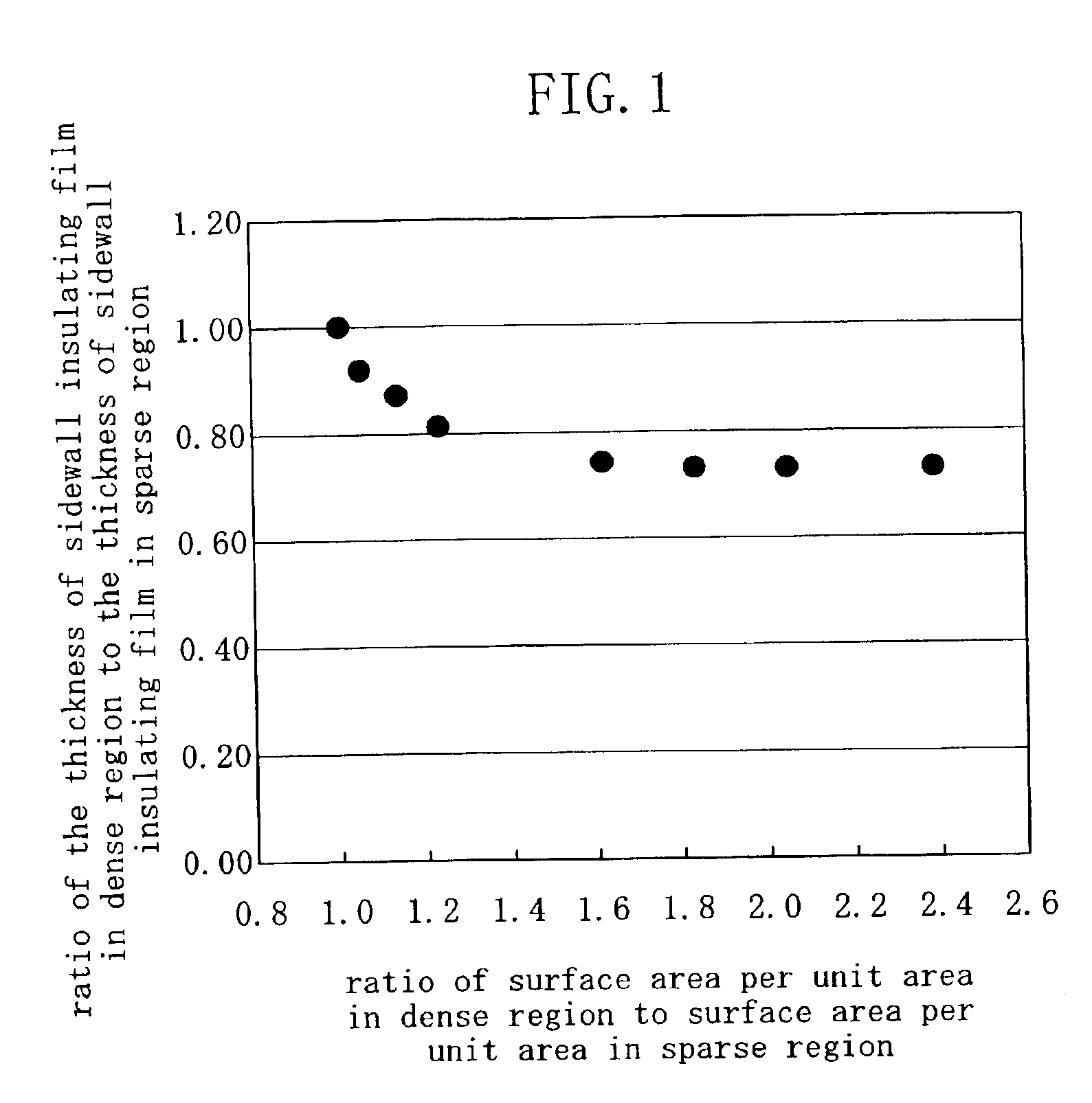
[0045]As has been described above, in the known method for fabricating a semiconductor device, if there are the dense region where the gate electrodes are densely arranged and the sparse region where the gate electrodes are sparsely arranged on the semiconductor substrate, the width of the sidewalls varies.
[0046]To prevent this variation, the present inventors thought that the width of the sidewalls varies because the deposition rate is determined by the feeding r...
embodiment 1
[0051
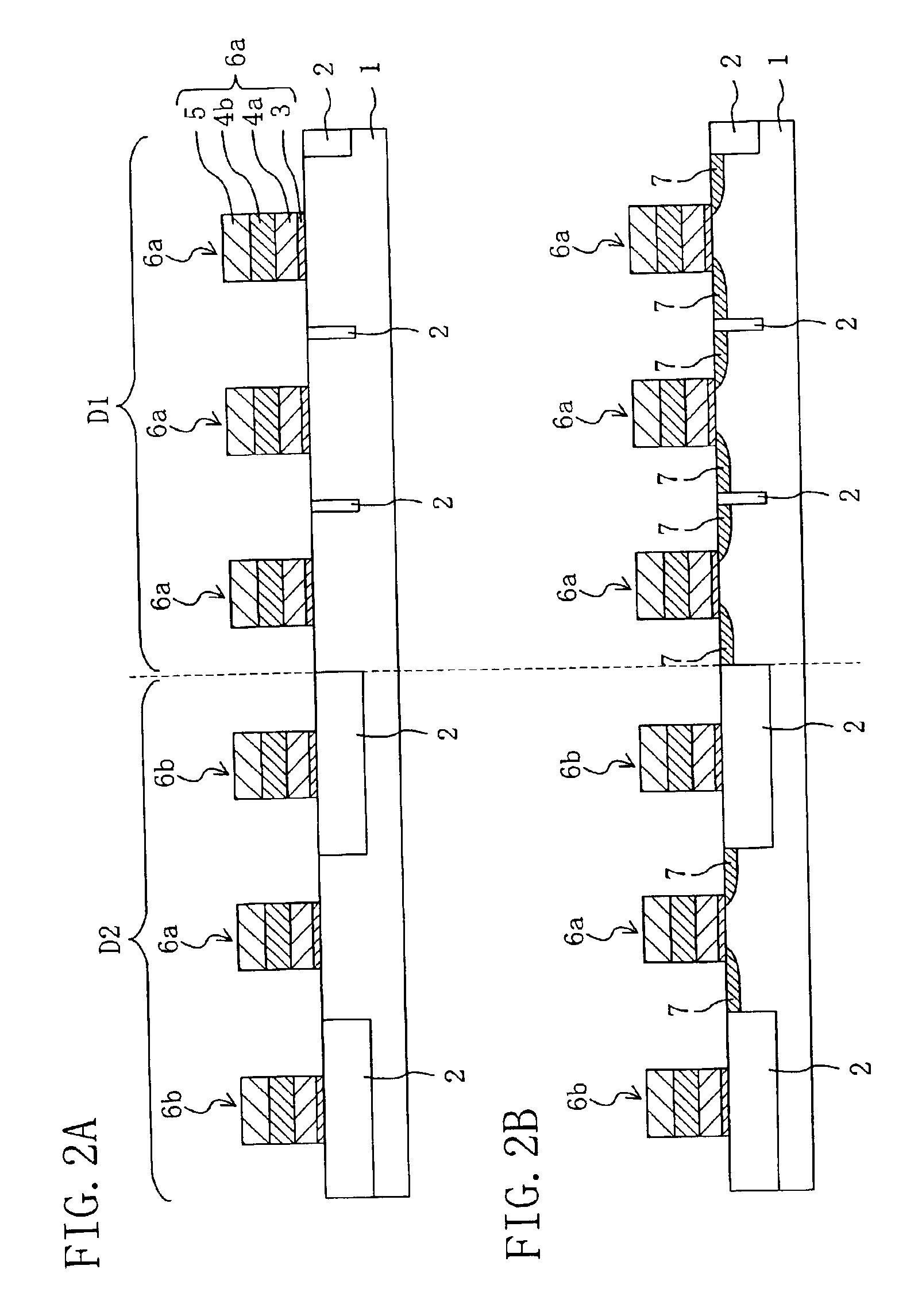
[0052]FIGS. 2A through 4B are cross-sectional views showing respective process steps for fabricating a semiconductor device according to a first embodiment of the present invention.
[0053]First, in a process step shown in FIG. 2A, isolation regions 2 each made of a trench isolation are formed in a semiconductor substrate 1. Then, thermal oxidation is performed in an NO / O2 atmosphere, thereby forming a silicon oxynitride film with a thickness of about 3 nm to be a gate insulating film. Thereafter, an undoped polysilicon film is deposited to a thickness of about 100 nm over the silicon oxynitride film. Subsequently, phosphorus (P) or boron (B) is implanted into part of the polysilicon film. Then, heat treatment is performed at 800° C. for 30 minutes so that phosphorus or boron is uniformly diffused in the polysilicon film, thereby making the polysilicon film p- or n-type. Then, after a natural oxide film formed on the polysilicon film has been removed, a multilayer metal film made...
embodiment 2
[0063
[0064]FIGS. 5A and 5B are cross-sectional views showing respective process steps for fabricating a semiconductor device according to a second embodiment of the present invention.
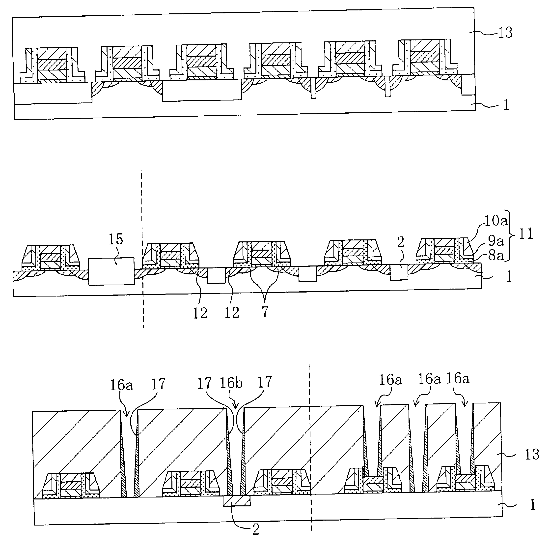
[0065]First, in a process step shown in FIG. 5A, isolation regions 2 each made of a trench isolation and a projecting isolation portion 15 are formed in a semiconductor substrate 1. Then, gate electrodes 6a each including: a gate insulating film 3 of a silicon oxynitride film; a lower gate electrode 4a of polysilicon; an upper gate electrode 4b of a multilayer metal film; and a gate protective layer 5 of a silicon nitride film, in that order from below, is formed.
[0066]In this embodiment, in the process step shown in FIG. 5A, the upper face of the semiconductor substrate 1 is divided into regions of 10×10 μm2, and the projecting isolation portion 15 whose height from the surface of the semiconductor substrate 1 is larger than that of the isolation regions 2 is formed in a sparse region D2 where the gate...
PUM
 Abstract
Description
Claims
Application Information