Digital semiconductor based smart surface

a digital semiconductor and smart surface technology, applied in the field of semiconductor based smart surface technology, can solve the problems of high cost associated with electrostatic printing process for commercial printing, rather slow process, and ink jet based printers are quite slow

Inactive Publication Date: 2005-07-28
VAIDYANATHAN NANDAKUMAR +1
View PDF0 Cites 1 Cited by
  • Summary
  • Abstract
  • Description
  • Claims
  • Application Information

AI Technical Summary

Benefits of technology

[0016] The present invention is directed toward forming a smart surface in which spatial locations on the surface can be digitally addressed and accessed for either reading or writing data from or to the particular spatial location on the surface. In particular, A smart surface includes a substrate having a top surface that has a smart surface element disposed within it. The smart surface element includes at least one conductive element that is electrically coupled to a memory circuit that can switch between a first state and a second state such that the conductive element has a state that corresponds to the associated memory circuit. The smart surface also includes an appliance having a bottom surface that has an electrical contact disposed within it and that physically proximate to the smart surface element and is also electrically connected to it. In this way, the electrical contact is able to receive the first and second state from the corresponding smart surface element.

Problems solved by technology

Since the entire image is constructed on a drop-by-drop basis, this can be a rather slow process.
In general, the oil loving areas of the image do not accept water and the water loving areas do not accept ink.
However, there are significant disadvantages with each of the methods.
For example, as previously mentioned, ink jet based printers are quite slow.
There are high costs associated with electrostatic printing processes for commercial printing, due to low throughput and inability to provide more than a certain number of copies (40,000 copies with current technology) on an electro-photography based machine, before the photoconductor drum is rendered useless for any other more reproduction.
In lithographic printing, primary costs include use of expensive printing plates or spools, and high costs for recycling and disposal of environmentally unfriendly chemicals.
Furthermore, the imaging or pre-imaging equipment used in the commercial printing world can be quite large and bulky.
However, the same large number of copies cannot be made because the charges wear off and need to be replenished.
In addition, the photoconductive drums lose sensitivity to spectral content after multiple usage.

Method used


Image

  • Digital semiconductor based smart surface
  • Digital semiconductor based smart surface
  • Digital semiconductor based smart surface

Examples


Embodiment Construction

[0046] Reference will now be made in detail to the preferred embodiments of the printing system, examples of which are illustrated in the accompanying drawings.

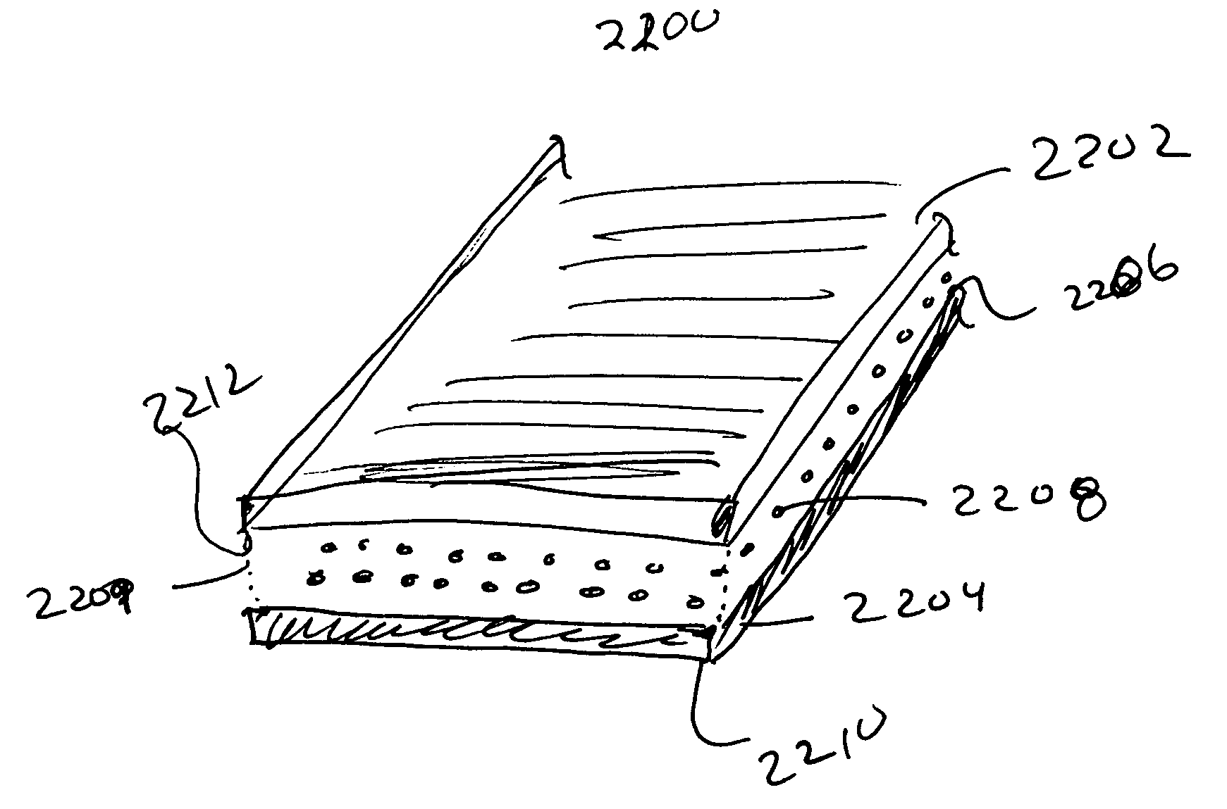
[0047] An electronic stored image based scheme is proposed which permits the digital printing elements to print a digitally stored image onto any medium. This is accomplished by using a semiconductor memory-based scheme in which an image is stored in an electronic memory with each digital printing element occupying one memory location. Since information is stored in memory as a voltage, by directly coupling the memory location to a conductive element, the stored voltage can be used to directly control whether or not conductive toner based inks are attracted to that conductive element.

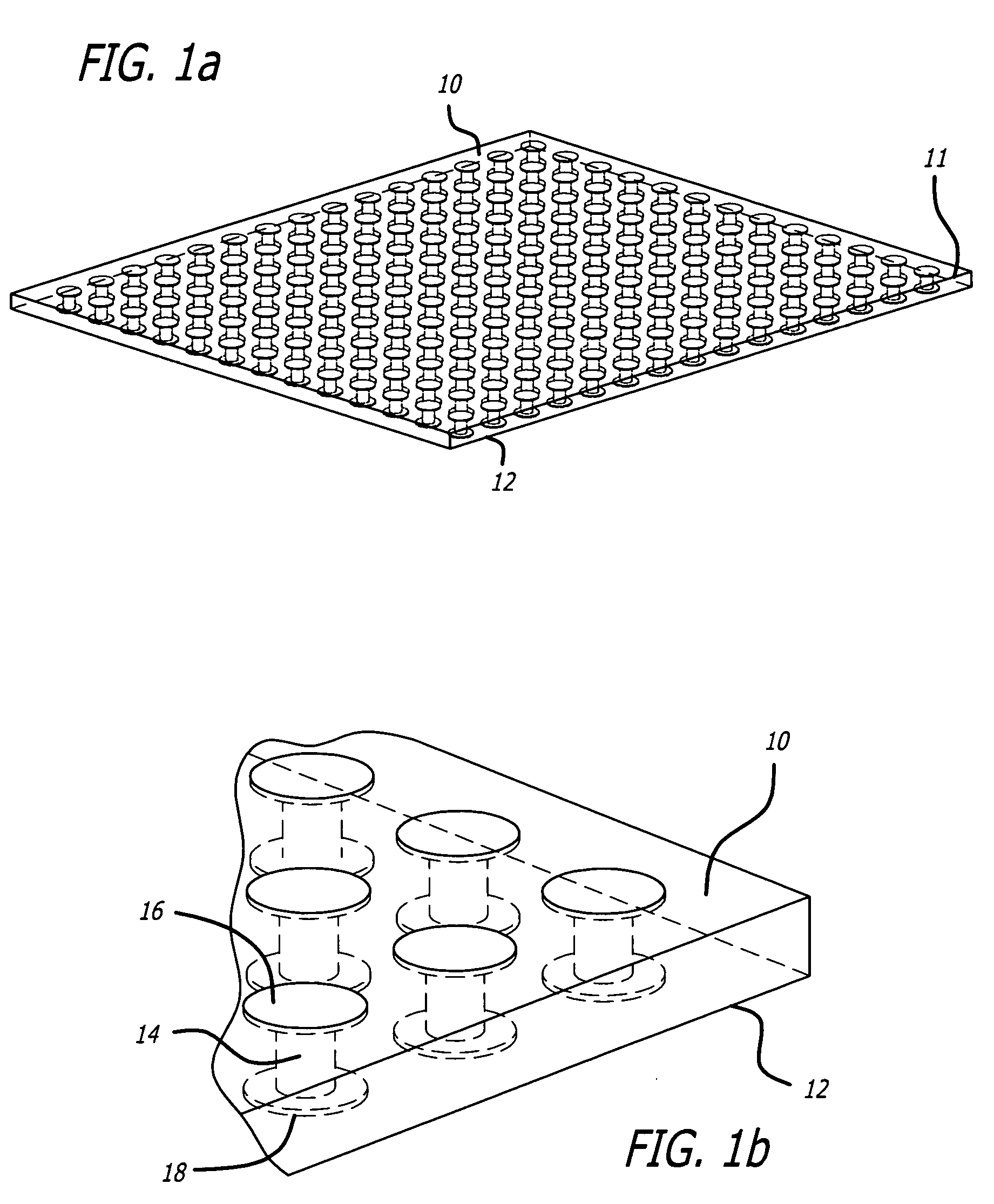
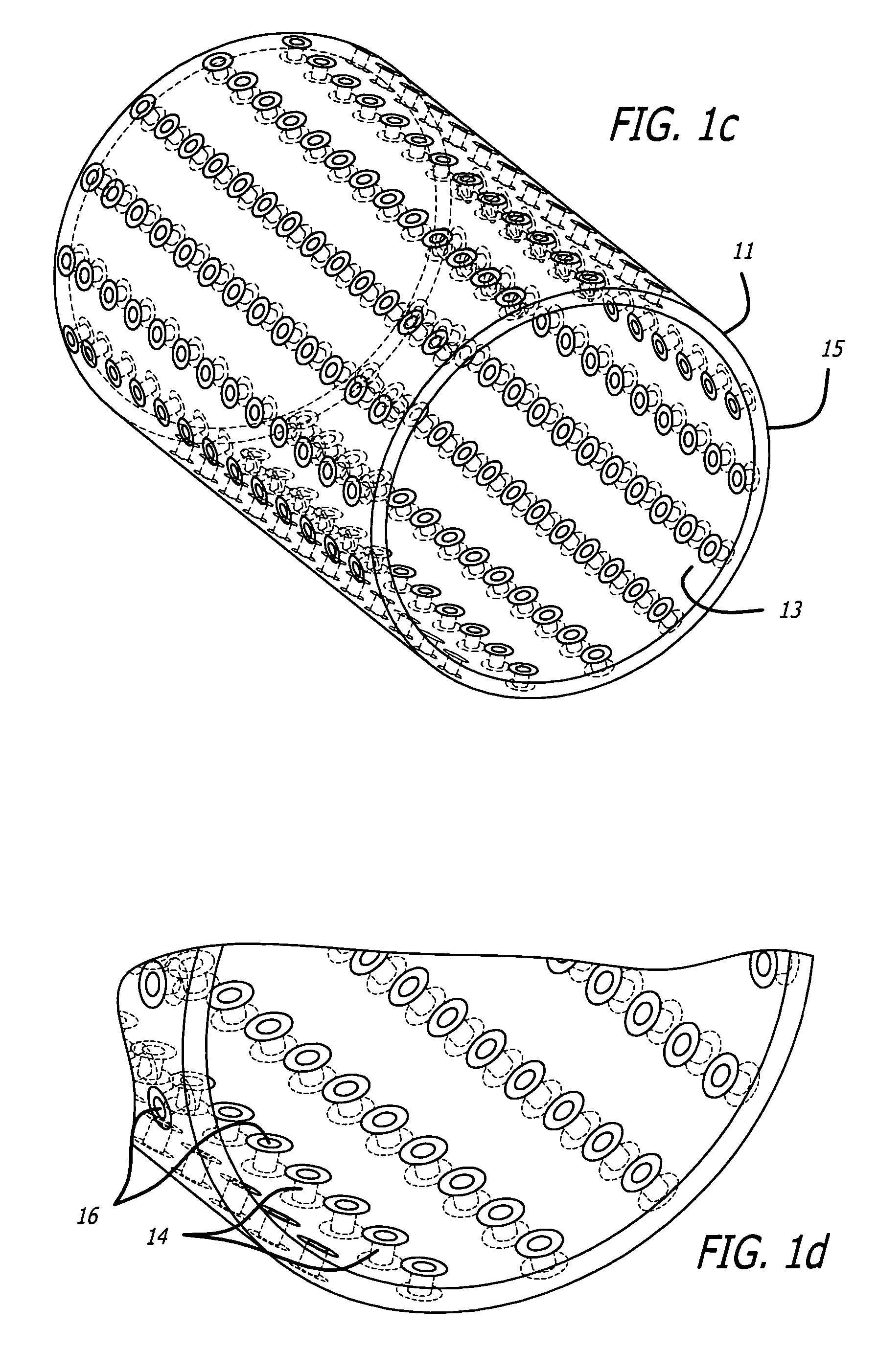
[0048] The system provides for a printing drum comprising a semiconductor memory. The semiconductor memory uses decoding elements to allow access to each of many storage locations without requiring an individual connection to each location. The...


PUM

PropertyMeasurementUnit
diameteraaaaaaaaaa
conductiveaaaaaaaaaa
electricalaaaaaaaaaa

Abstract

A smart surface is composed of a semiconductor memory layer overlaid on an insulated conductive layer with a one to one correspondence of each memory cell with the conductive pad on the insulated layer. The entire structure can be fashioned into a either a planar structure or other geometric structure. An appliance may be overlaid the smart surface and signals transmitted and received to and from the appliance via the conductive pad(s) of the smart surface.

Description

[0001] This application claims priority to the prior patent application entitled, DIGITAL SEMICONDUCTOR BASED PRINTING SYSTEM AND METHOD, having a Ser. No. 10 / 759,765 and that was filed in the United States Patent and Trademark Office on Jan. 16, 2004.BACKGROUND [0002] 1. Field of the Invention [0003] The present invention generally relates to semiconductor techniques for forming a smart surface. [0004] 2. General Background and State of the Art [0005] There are currently several dominant techniques used in computer based and commercial printing (non-impact printing). [0006] A large portion of Personal Computer (PC) based printing is based on Ink Jet technology, or “Drop on Demand” methods where the image to be printed is constructed on an appropriate printing medium such as paper, plastic, textiles, printing plates and even silicon based substrates using print heads which eject drops of ink at the appropriate location on the printing medium. Since the ejection of ink occurs at the ...

Claims


Application Information

Patent Timeline
Patent Type & Authority Applications(United States)
IPC IPC(8): B41J2/385B41M1/42B41M5/00B41N1/00G03G5/00G03G15/34
CPCB41M1/00B41M1/04G03G15/6591G03G15/34G03G2215/00523G03G5/00
Inventor VAIDYANATHAN, NANDAKUMARSUBRAHMANYAN, RAVI
Owner VAIDYANATHAN NANDAKUMAR
Why Eureka
Try Eureka