Semiconductor memory device and method of operating same
a memory device and semiconductor technology, applied in semiconductor devices, digital storage, instruments, etc., can solve the problems of complex and expensive integration of one capacitor memory cells into logic devices, the source or drain region of a non-symmetrical device is typically not interchangeable, and the device is limited or restricted in the size of the memory cell
- Summary
- Abstract
- Description
- Claims
- Application Information
AI Technical Summary
Benefits of technology
Problems solved by technology
Method used
Image

Examples
second embodiment
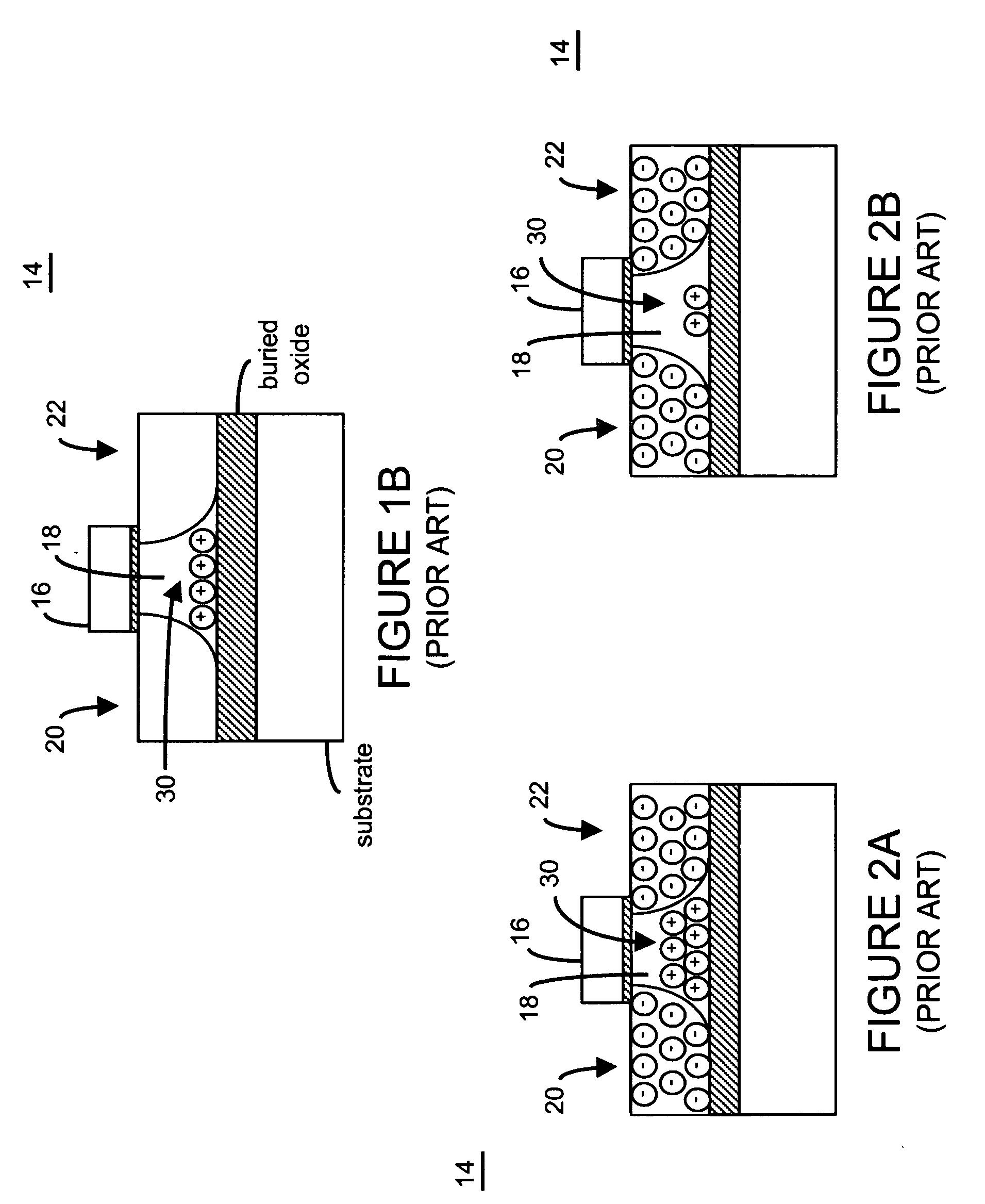
[0059] In a second embodiment, with reference to FIGS. 1 and 5, transistor 14 (a 0.25 micron N-channel MOSFET DRAM cell) may be operated using the exemplary voltage values indicated. In this regard, to write a logic high (binary data state “1”), a strong accumulation of majority carriers at the interface of gate oxide 32 and floating body region 18 is required. In one exemplary embodiment, a voltage of −1.7V is applied to gate 16 and a voltage of 1.7V is applied to drain region 22 to provide the strong accumulation of majority carrier at the interface of gate oxide 32 and floating body region 18. These control signals cause deformation of the valence and conduction bands at the interface between body region 18 and source region 20. As a result, minority carriers (here, electrons) are injected into the conduction band by means of a tunnel effect (an effect known as gate induced drain leakage (GIDL)), which in turn causes the generation of majority carriers (here, holes) in body regio...
third embodiment
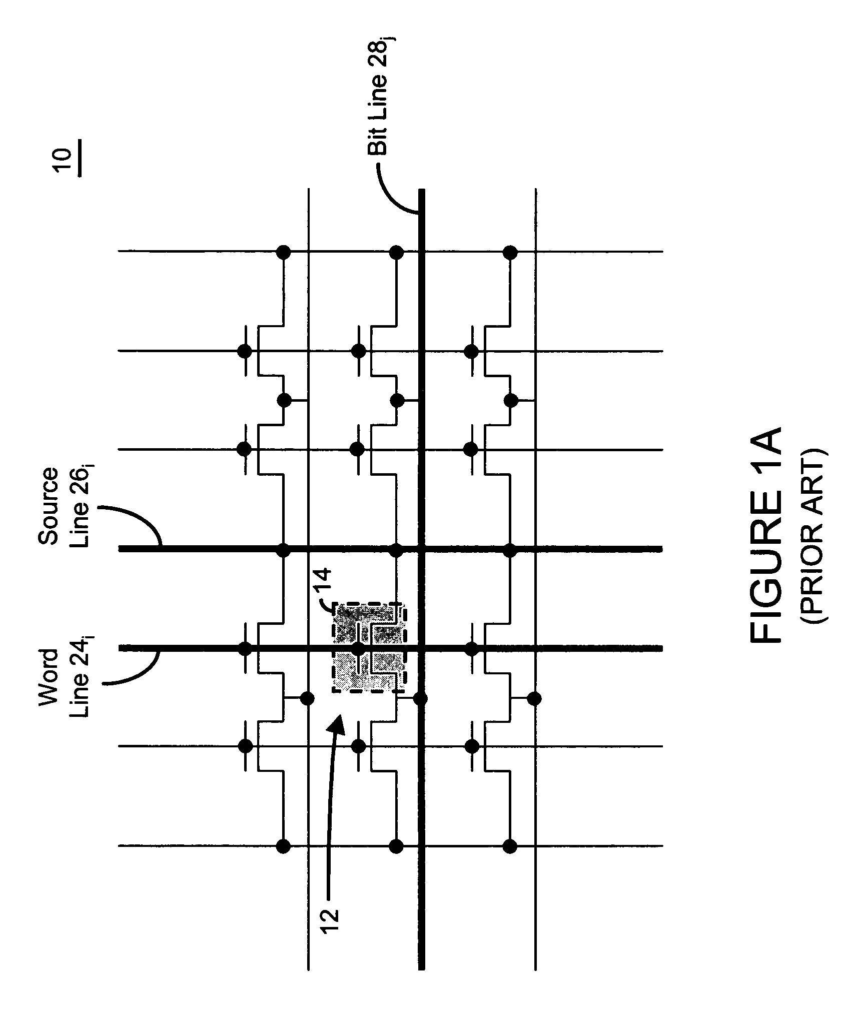
[0061] In a third embodiment, with reference to FIGS. 1 and 6, transistor 14 (a 0.13 micron technology DRAM cell) may be programmed and / or operated using the exemplary voltages indicated. The voltages set forth in FIG. 6 represent “ideal” conditions, in which the application of the voltage pulses does not disturb the data stored within the cell. However, the cells are arranged in matrices in which some cells are accessed when others remain un-accessed, and column and row decoding are therefore necessary to enable the matrices to function. This results in voltage levels differing from the levels being applied during write, read and hold operations (in practice, all of the cells that share either the same column or row with the addressed memory cell), as a consequence of which disturbance of the data stored within those cells may occur.
[0062] An example of this is shown in FIGS. 1 and 7, in which data state “0” is being written to memory cell 12 at the intersection of the selected wor...
PUM
 Abstract
Description
Claims
Application Information