Back-contact solar cells and methods for fabrication

a solar cell and back contact technology, applied in the field of back contact solar cell manufacturing methods, can solve the problems of low-cost process sequence, add complexity and cost, and increase the complexity of the manufacturing process, and achieve the effect of improving and simplifying the method of production and reducing costs

Inactive Publication Date: 2005-08-11
APPLIED MATERIALS INC
View PDF99 Cites 205 Cited by
  • Summary
  • Abstract
  • Description
  • Claims
  • Application Information

AI Technical Summary

Benefits of technology

[0025] A primary advantage of the present invention is that it provides improved and simpler methods of producing EWT solar cells at a decreased cost.
[0026] Yet another advantage of the present invention is that it provides methods wherein conductive vias and associated grid lines on the rear surface, and optionally dopant lines on the front surface, are more heavily doped with an n+-dopant, preferably phosphorus, than are the remaining surface areas.
[0027] Other objects, advantages and novel features, and further scope of applicability of the present invention will be set forth in part in the detailed description to follow, taken in conjunction with the accompanying drawings, and in part will become apparent to those skilled in the art upon examination of the following, or may be learned by practice of the invention. The objects and advantages of the invention may be realized and attained by means of the instrumentalities and combinations particularly pointed out in the appended claims.
[0028] The accompanying drawings, which are incorporated into and form a part of the specification, illustrate one or more embodiments of the present invention and, together with the description, serve to explain the principles of the invention. The drawings are only for the purpose of illustrating one or more preferred embodiments of the invention and are not to be construed as limiting the invention. In the drawings:
[0029]FIG. 1 is an illustration of a generic back-contact solar cell 10.
[0030]FIG. 2A is a cross-section of a silicon wafer that has been drilled and etched in a back-contact cell process sequence of the invention, and FIG. 2B is a top view of a portion of the wafer of FIG. 2A.

Problems solved by technology

However, this approach adds significant complexity to the manufacturing process and is accordingly more expensive.
However, this also adds complexity and cost.
A critical issue for any back-contact silicon solar cell is developing a low-cost process sequence that also electrically isolates the negative and positive polarity grids and junctions.
The technical issue includes patterning of the doped layers (if present), passivation of the surface between the negative and positive contact regions, and application of the negative and positive conductivity contacts.

Method used


Image

  • Back-contact solar cells and methods for fabrication
  • Back-contact solar cells and methods for fabrication
  • Back-contact solar cells and methods for fabrication

Examples


Embodiment Construction

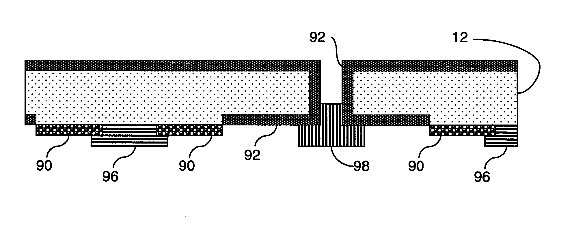
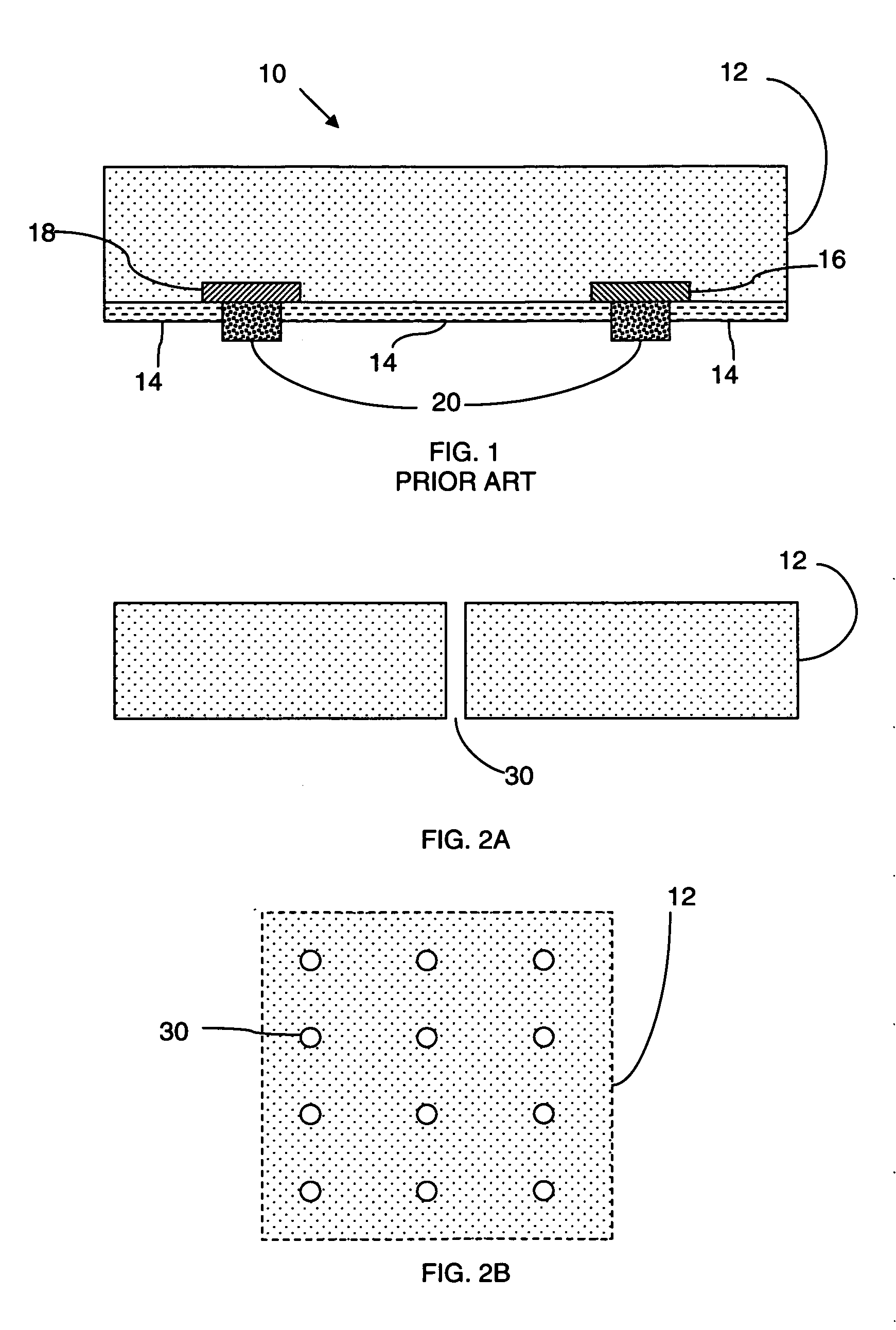
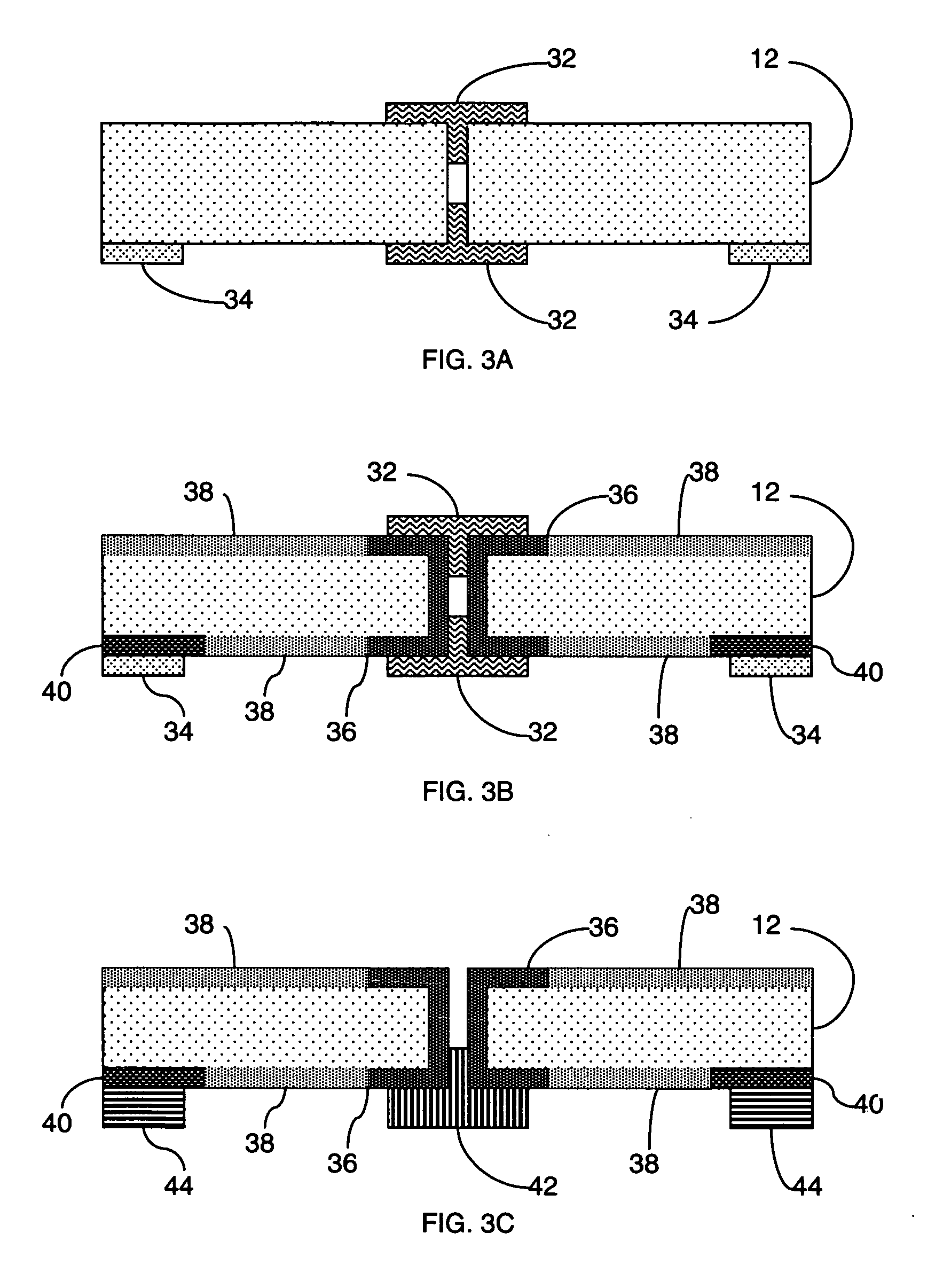
[0036] The invention disclosed herein provides for improved methods and processes for fabrication of back-contact solar cells, particularly methods and processes providing for simpler, more reliable and more economical fabrication. It is to be understood that while a number of different discrete methods are disclosed, one of skill in the art could combine or vary two or more methods, thereby providing an alternative additional method of fabrication. It is also to be understood that while the figures and example process sequences describe fabrication of back-contact EWT cells, certain of these process sequences can be used for fabrication of other back-contact cell structures such as MWT, MWA, or back-junction solar cells. In particular, the methods under the headings ““Use of Printed Diffusion Barriers and Dopant Diffusion Barriers” and “Use of Spin-On Glass Diffusion Barrier” and “Use of Spin-On Glasses as Diffusion Barrier and Dopant Sources” can be directly applied to any back-co...


PUM


Abstract

Methods for fabrication of emitter wrap through (EWT) back-contact solar cells and cells made by such methods. Certain methods provide for higher concentration of dopant in conductive vias compared to the average dopant concentration on front or rear surfaces, and provided increased efficiency. Certain methods provide for selective doping to holes for forming conductive vias by use of printed dopant pastes. Other methods provide for use of spin-on glass substrates including dopant.

Description

CROSS-REFERENCE TO RELATED APPLICATIONS [0001] Related applications entitled “Contact Fabrication of Emitter Wrap-Through Back Contact Silicon Solar Cells”, by Peter Hacke and James M. Gee, U.S. Utility Patent Application Attorney Docket No. 31474-1005-UT, and entitled “Buried-Contact Solar Cells With Self-Doping Contacts”, by James M. Gee and Peter Hacke, U.S. Utility Patent Application Attorney Docket No. 31474-1004-UT, are being filed concurrently herewith, and the specification of each is incorporated herein by reference. [0002] This application claims the benefit of the filing of U.S. Provisional Patent Application Serial No. 60 / 542,390, entitled “Fabrication of Back-Contact Silicon Solar Cells”, filed on Feb. 5, 2004, and of U.S. Provisional Patent Application Serial No. 60 / 542,454, entitled “Process for Fabrication of Buried-Contact Cells Using Self-Doping Contacts”, filed on Feb. 5, 2004, and the specifications thereof are incorporated herein by reference.BACKGROUND OF THE I...

Claims


Application Information

Patent Timeline
Patent Type & Authority Applications(United States)
IPC IPC(8): H01L21/00H01L31/068
CPCH01L31/03529H01L31/068Y02E10/547H01L31/022458Y10S438/928H01L31/1804H01L31/0682Y02P70/50H01L31/04H01L31/18
Inventor GEE, JAMES M.HACKE, PETER
Owner APPLIED MATERIALS INC
Why Eureka
Try Eureka