Semiconductor device

a semiconductor and device technology, applied in the field of semiconductor devices, can solve the problems affecting the compactness of the information appliance, and certain risks of operation failure, so as to achieve the effect of reducing the temperature of the semiconductor device when it is operated

Inactive Publication Date: 2005-09-01
HITACHI LTD +1
View PDF4 Cites 72 Cited by
  • Summary
  • Abstract
  • Description
  • Claims
  • Application Information

AI Technical Summary

Benefits of technology

[0012] In accordance with the present invention, the temperature increase when the semiconductor device is operated can be reduced.

Problems solved by technology

On the other hand, mounting areas of these semiconductor memories are increased in connection with large memory capacities, which may cause a certain factor to impede compactnesses of these information appliances.
As a result, there are certain risks as to operation failures and destruction of semiconductor elements, which are caused by temperature increases during operations of the semiconductor devices.

Method used


Image

  • Semiconductor device
  • Semiconductor device
  • Semiconductor device

Examples


first embodiment

[0029] Referring now to FIG. 1 to FIG. 6J, a description is made of a structure of a semiconductor device according to the present invention. In the below-mentioned description, such a semiconductor memory in which DRAMs have been stacked is exemplified as the semiconductor device.

[0030] First, an entire structure of the semiconductor device according to this first embodiment will now be described.

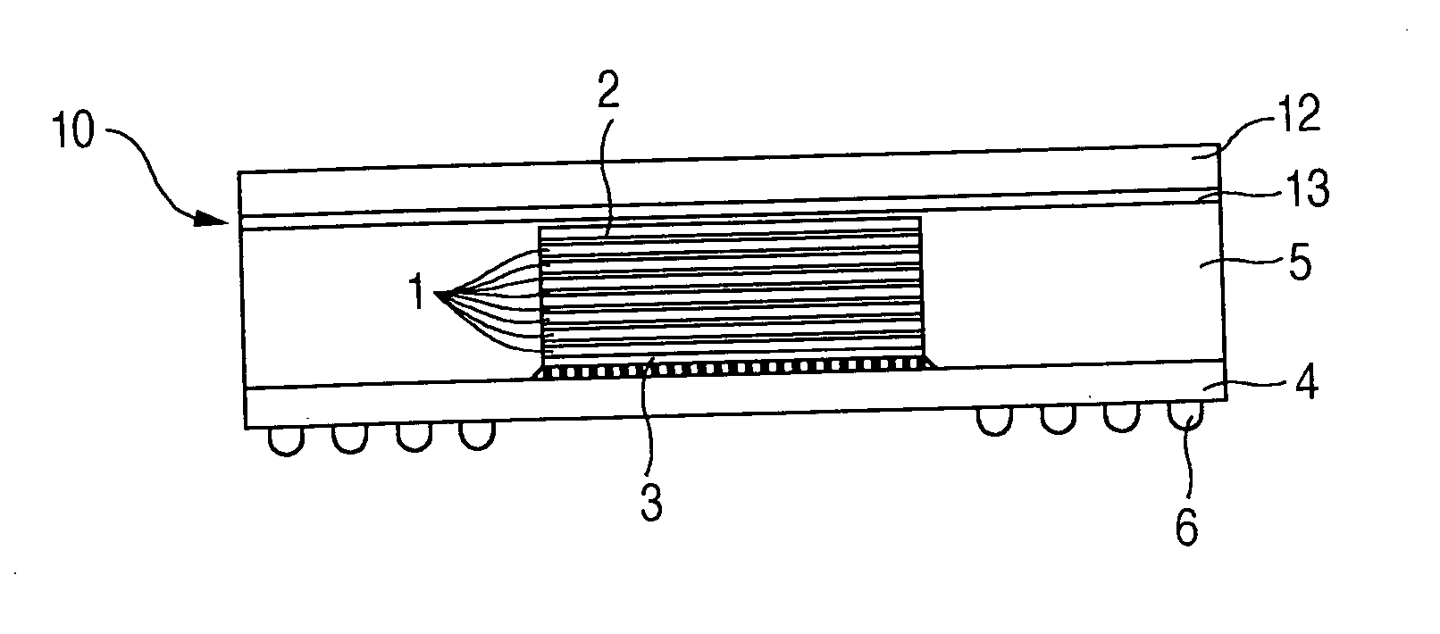
[0031]FIG. 1 is a sectional side view for showing an entire structure of the semiconductor device 10 according to the first embodiment of the present invention.

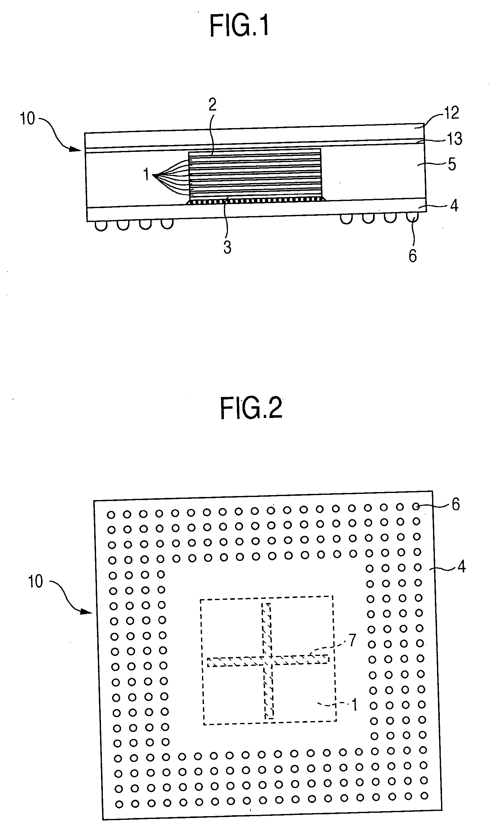
[0032]FIG. 2 is a bottom view for representing an entire structure of the semiconductor device 10 according to the first embodiment of the present invention.

[0033] As indicated in FIG. 1, this semiconductor device 10 is constituted by 8 sheets of DRAM chips 1, an interface chip 2, an “Si” interposer 3 and a resin substrate interposer 4. The DRAM chips 1 have been stacked on each other. The interface chip 2 is arranged on an upper...

second embodiment

[0081] Referring now to FIGS. 7A and 7B, a description is made of a structure of a semiconductor device 10A according to the present invention.

[0082]FIG. 7A and FIG. 7B are structural diagrams for showing an entire structure of the semiconductor device 10A according to the second embodiment of the present invention. FIG. 7A is a sectional side view are FIG. 7B is a bottom view of the semiconductor device 10A. It should be noted that the same reference numerals shown in FIG. 1 and FIG. 2 will be employed as those for indicating the same structural portions shown in FIG. 7A and FIG. 7B.

[0083] In the semiconductor device 10A of this second embodiment, not only solder balls 6 are provided at peripheral portions of a bottom plane of DRAM chips 1, but also, solder balls 6A which are used to join a resin substrate interposer 4 to a module board are provided just under a center portion of the DRAM chips 1.

[0084] In the case that the solder balls 6A are arranged just under the DRAM chips 1...

third embodiment

[0086] Next, a description is made of a structure of a semiconductor device 10B according to the present invention with reference to FIG. 8A and FIG. 8B.

[0087]FIG. 8A and FIG. 8B are structural diagrams for indicating entire structures of the semiconductor device 10B according to the third embodiment of the present invention; FIG. 8A is a sectional side view and FIG. 8B is a bottom view of the entire structures. It should be noted that the same reference numerals shown in FIG. 1 and FIG. 2 are employed as those for indicating the same structural portions shown in FIG. 8A and FIG. 8B.

[0088] In the semiconductor device 10B of this third embodiment, solder balls 6B are arranged over the entire lower plane of a resin board interposer 4. As explained above, in such a case that the solder balls 6B are arranged over the entire lower plane of the resin substrate interposer 4, a large shearing deformation load is produced by a thermal deformation in the solder balls 6B which are arranged ar...


PUM


Abstract

A semiconductor device capable of reducing a temperature increase during operation thereof is provided. In the semiconductor device, an interface chip is stacked on a plurality of stacked semiconductor elements. Both an “Si” interposer and a resin interposer are arranged under the plural semiconductor elements. The Si interposer is arranged between the resin interposer and the plural semiconductor elements. The Si interposer owns a thickness which is thicker than a thickness of a semiconductor element, and also has a linear expansion coefficient which is smaller than a linear expansion coefficient of the resin interposer, and further, is larger than, or equal to linear expansion coefficients of the plural semiconductor elements.

Description

BACKGROUND OF THE INVENTION [0001] The present invention generally relates to a semiconductor device. More specifically, the present invention is directed to a semiconductor device suitably designed for mounting a plurality of semiconductor elements in a stack manner. [0002] Semiconductor devices, especially, semiconductor memories have been used in various sorts of information appliances such as large-scaled computers, personal computers, and portable appliances, while memory capacities required thereof are increased year by year. On the other hand, mounting areas of these semiconductor memories are increased in connection with large memory capacities, which may cause a certain factor to impede compactnesses of these information appliances. Under such a circumstance, various techniques capable of mounting semiconductor memories in high mounting density have been developed. As techniques capable of realizing memories having large storage capacities within limited mounting areas, for...

Claims


Application Information

Patent Timeline
Patent Type & Authority Applications(United States)
IPC IPC(8): H01L23/48H01L25/18H01L25/065H01L25/07H01L25/10
CPCH01L23/481H01L25/0657H01L2924/10253H01L2924/01087H01L2924/01019H01L24/48H01L2924/19105H01L2924/19041H01L2924/15312H01L2924/15311H01L2924/01079H01L2224/16145H01L2224/16225H01L2224/48091H01L2224/48227H01L2224/48472H01L2224/73204H01L2225/06513H01L2225/0652H01L2225/06541H01L2225/06589H01L2225/06593H01L2924/00014H01L2924/00H01L2224/45144H01L2924/14H01L2224/05573H01L2224/13025H01L2224/05647H01L2924/181H01L24/16H01L2924/00012H01L2224/45099H01L2224/45015H01L2924/207H01L25/10
Inventor TANIE, HISASHIHISANO, NAEOHTA, HIROYUKIIKEDA, HIROAKIANJOH, ICHIROKATAGIRI, MITSUAKIWATANABE, YUJI
Owner HITACHI LTD
Why Eureka
Try Eureka