Self-biased darlington amplifier

a darlington amplifier and self-biased technology, applied in the direction of amplifiers, amplifiers with semiconductor devices only, amplifiers, etc., can solve the problems of reducing the output voltage and rf headroom provided to the darlington output stage, reducing the maximum output power capability, etc., to improve output power efficiency and linearity, increase the voltage supplied, and reduce the effect of temperature sensitivity

Inactive Publication Date: 2005-09-01
QORVO US INC
View PDF6 Cites 10 Cited by
  • Summary
  • Abstract
  • Description
  • Claims
  • Application Information

AI Technical Summary

Benefits of technology

[0016] The objects, features and advantages of the present invention include providing self-biased Darlington amplifier that may (i) increase the voltage supplied to an output device, (ii) improve output power efficiency and linearity, (iii) reduce the temperature sensitivity (e.g., by a factor of 2 over conventional approaches), (iv) reduce the supply voltage sensitivity (e.g., by a factor of 2 over conventional approaches), (v) enable dynamic bias operation (e.g., class AB or B), (vi) be monolithically integrated to reduce size and / or cost, and / or (vii) be applied to 3.3V SiGe HBT and Si BJT Darlington gain blocks.

Problems solved by technology

However, the DC bias set resistor RDC also creates a voltage drop, reducing the output voltage and RF headroom provided to the Darlington output stage.
Moreover, for class AB, B, and C operation (e.g., where the current Icc increases with input power), the resistor RDC will drop even more voltage, reducing the maximum output power capability.

Method used


Image

  • Self-biased darlington amplifier
  • Self-biased darlington amplifier
  • Self-biased darlington amplifier

Examples


Embodiment Construction

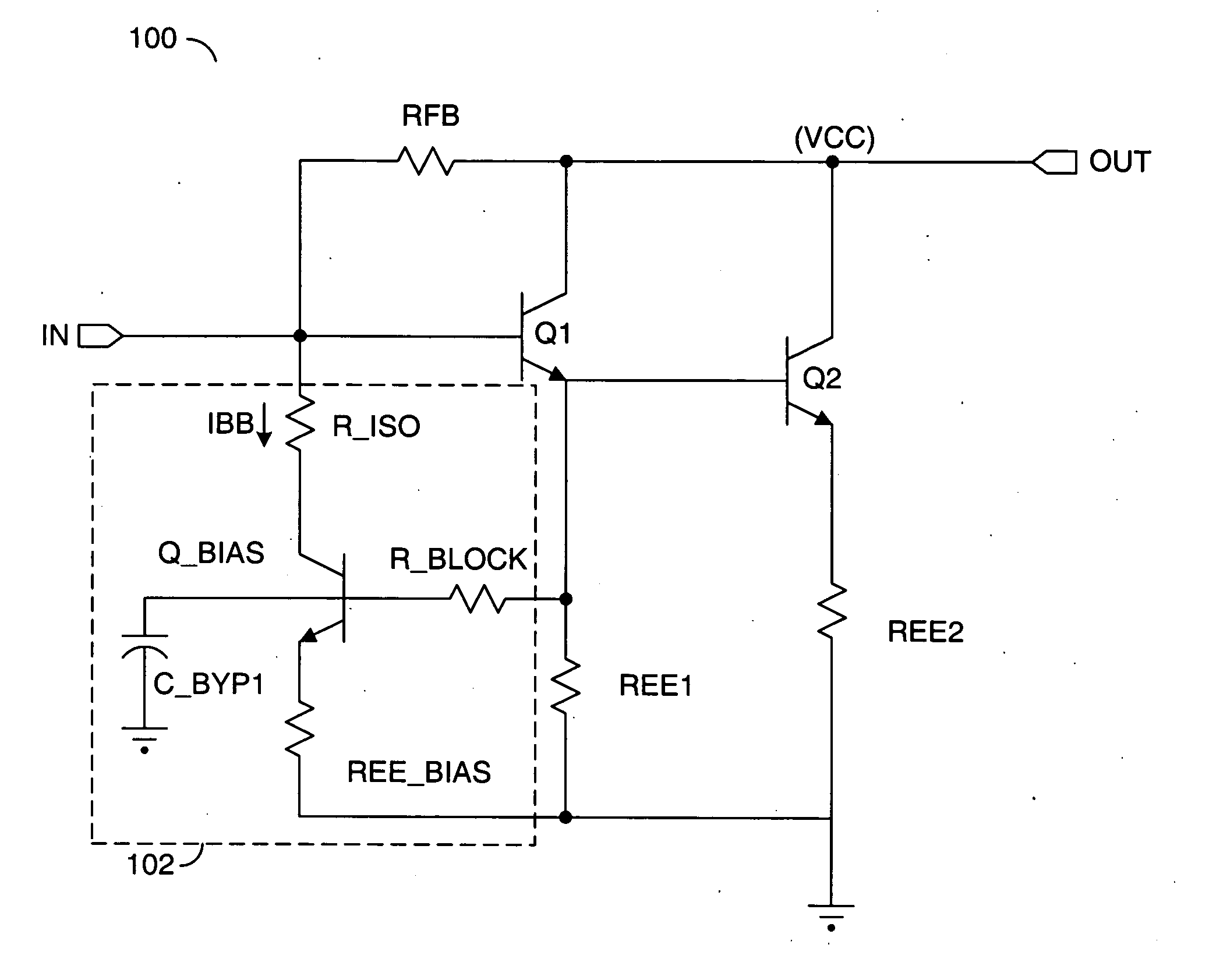
[0032] The present invention may implement a self-bias Darlington Gain Block that may (i) eliminate a bias resistor (e.g., RDC), (ii) increase output voltage headroom, (iii) improve stability over temperature and supply voltage (e.g., Vcc) variations, and / or (iv) enable class AB biasing. In one example, the present invention may be implemented in a SOT-89 package. However, other packages, such as other 3-pin packages, may be implemented to meet the design criteria of a particular implementation.

[0033] Referring to FIG. 6, a diagram of a circuit 100 illustrating a preferred embodiment of the present invention is shown. The circuit 100 generally comprises a Darlington gain block 102, a capacitor (e.g., C_BYPASS) and an inductor 104. The inductor 104 may provide a radio frequency (RF) choke. The Darlington gain block 102 generally presents a signal (e.g., OUT) in response to a signal (e.g., IN) and a current presented through the inductor 104. The circuit 100 is implemented without th...


PUM


Abstract

An apparatus comprising a Darlington transistor pair and a bias circuit. The Darlington transistor pair may be configured to generate an output signal at an output node in response to an input signal received through an input node. The bias circuit may be coupled between an output transistor of said Darlington transistor pair and the input node. The bias circuit generally comprises (a) a bias transistor, (b) a bypass capacitor, and (c) a resistor connected between a base of the bias transistor and base of the output transistor.

Description

[0001] This is a continuation of U.S. Ser. No. 10 / 623,070, filed Jul. 18, 2003.FIELD OF THE INVENTION [0002] The present invention relates to amplifiers generally and, more particularly to a method and / or architecture for implementing a self-biased Darlington amplifier. BACKGROUND OF THE INVENTION [0003] Conventional Darlington Amplifiers are often employed in a 3 terminal package (i.e., a SOT-89 package) or other 3 terminal style transistor package. Such amplifier packages are attractive because they typically have a small outline, a low cost, and a user-friendly implementation. Conventional 3-terminal transistor style packages typically allow one RF input, one RF output, and one reference ground terminal. The limited number of terminals imposes a constraint for bias solutions in Darlington amplifiers. [0004] Referring to FIG. 1, a circuit 10 illustrating a conventional Darlington gain block biasing scheme is shown. In the circuit 10, an off-chip bias set Resistor RDC is used to se...

Claims


Application Information

Patent Timeline
Patent Type & Authority Applications(United States)
IPC IPC(8): H03F1/30H03F3/04H03F3/343
CPCH03F1/302H03F3/3435H03F3/04
Inventor KOBAYASHI, KEVIN W.
Owner QORVO US INC
Why Eureka
Try Eureka