Two-step switch

a two-step switch and switch body technology, applied in the direction of switch side location, contact surface shape/structure, movable contacts, etc., can solve the problems of difficult to provide such different levels on the printed circuit board, the size of the switch would become larger, and the inability to provide a small-size two-step switch

Inactive Publication Date: 2005-09-15
FUJI ELECTRONICS IND
View PDF9 Cites 19 Cited by
  • Summary
  • Abstract
  • Description
  • Claims
  • Application Information

AI Technical Summary

Benefits of technology

[0016] It is an object of the present invention to provide a two-step switch, which can be minimized by preventing the increase of size in radial direction. Further, it is another object of the present invention to provide the two-step switch which can be used for printed circuit board easily.
[0027] As discussed above, the two-step switch according to the present invention has the circuit board, having the first fixed contacts, the second fixed contact and the third fixed contact, the first contact spring, having the outer peripheral contacts in regular contact with the first fixed contacts of the circuit board, and also having the inner contact positioned inside of the outer peripheral contacts and is reversed by depressing operation, and the second contact spring, stacked on the first contact spring via the first insulation sheet, having the outer peripheral contact in regular contact with the second fixed contact of the circuit board, and also having the inner contact positioned inside of the outer peripheral contact and is reversed by depressing operation. Since the first contact spring and the second contact spring are stacked, the size in radial direction may be reduced, whereby it is possible to incorporate in a narrow space.
[0028] In particular, with reference to a portable telephone as an example, the thickness has been reduced, thus the size of the side surface should be minimized. As the size in radial direction of the two-step switch according to the prior art is large, it is quite difficult to incorporate the conventional two-step switch in such a narrow space. On the other hand, according to the two-step switch of the present invention, because the size in radial direction is reduced, it is possible to be incorporated in such a narrow space easily.
[0030] Preferably, the first contact spring may be in a dome shape, of which both ends of outer peripheral parts, opposing to each other, serve as the outer peripheral contacts, and of which protruding part having the inner contact has been formed in a bridge shape with having the openings formed on the both sides, and the both ends of outer peripheral parts have been formed in bowing shapes toward the opposite side of the protruding part. With this structure, it is possible to secure the height, i.e., the stroke, whereby the different levels are no more required on the fixed contacts, and it is possible to cope with various printed circuit boards.
[0031] Preferably, the both ends of outer peripheral parts may have the projecting chips formed and projecting in radial direction and toward the opposite side of the protruding part, and the projecting chips serve as the outer peripheral contacts. With this structure, the above effect may be further improved.

Problems solved by technology

However, the conventional two-step switch according to the above disclosure has several disadvantageous points.
Consequently, the size of switch would become larger in radial direction, and it is impossible to provide a small-size two-step switch.
However, it is very difficult to provide such different levels on a printed circuit board, hence, the switch contact spring 201 according to the prior art cannot be used by simply making in contact with the printed circuit board.
Third, when the conventional switch is used for the printed circuit board, the switch contact spring 201 must be soldered, thus the switch should be made of any durable material against high temperature, which would increase the production cost.
Fourth, according to the switch contact spring 201 as shown in FIG. 18, two different loading characteristics must be provided by the single contact spring, which would require difficult adjustment working, having poor flexibility to be applied to various specifications.

Method used


Image

  • Two-step switch
  • Two-step switch
  • Two-step switch

Examples


first embodiment

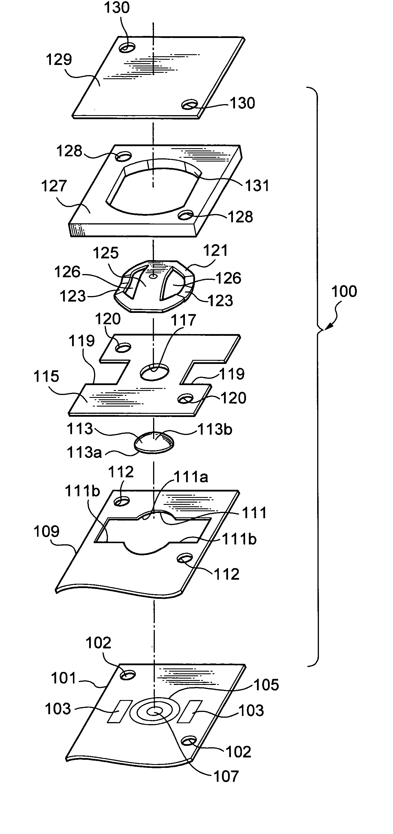
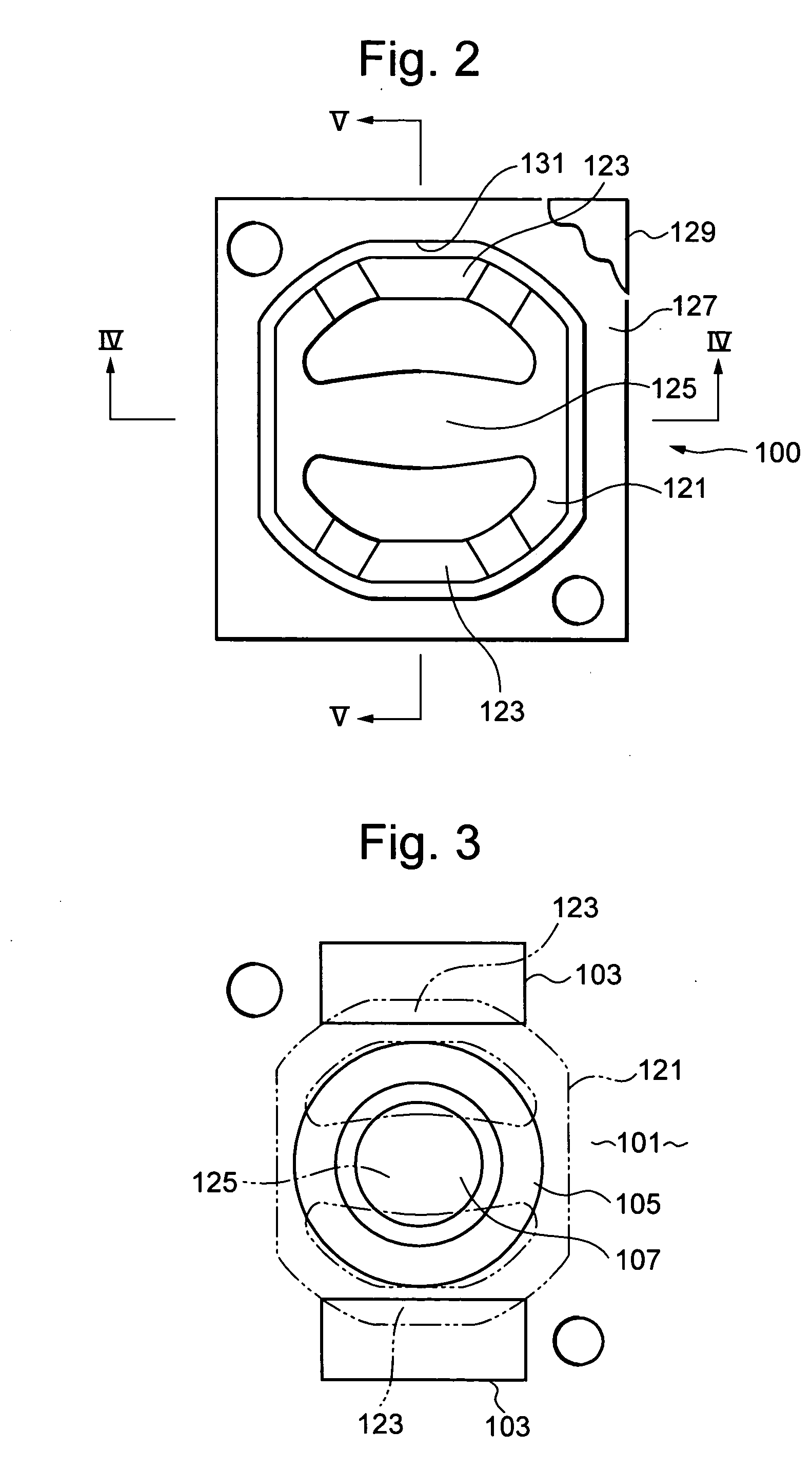
[0053] A first embodiment of the present invention will now be described with reference to FIGS. 1 through 9. FIG. 1 is an exploded perspective view of a two-step switch 100 according to the first embodiment, FIG. 2 is a plan view of the two-step switch 100, FIG. 3 is a plan view of a printed circuit board, FIG. 4 is a sectional view as seen by the line IV-IV of FIG. 2, and FIG. 5 is a sectional view as seen by the line V-V of FIG. 2.

[0054] As illustrated in FIGS. 1 and 3, there is a printed circuit board 101, on which, first fixed contacts 103, a second fixed contact 105, and a third fixed contact 107, are provided. The printed circuit board 101 has penetrating holes 102, 102, at positions diametrically opposite to each other, into which fixing screws (not shown) are inserted respectively.

[0055] Further, as illustrated in FIGS. 1, 4 and 5, there is an adhesive sheet 109, serving as a second insulation sheet, positioned above the printed circuit board 101. The adhesive sheet 109 h...

second embodiment

[0072] A second embodiment of the present invention will now be described with reference to FIG. 10. According to the second embodiment, the both ends of the first contact spring 121 according to the first embodiment are formed in bowing shapes toward the lower side, at which projecting chips are provided, respectively serving as the outer peripheral contacts 123, 123. As illustrated in FIG. 10, the outer peripheral contacts 123, 123 project, not only in radial direction, but also toward the opposite side of the protruding part. Thus, it is further possible to secure the height, in particular the stroke.

[0073] The other structure is substantially the same as that of the first embodiment, so the identical reference numerals are given to the identical parts, and the detailed explanation will not be done here.

third embodiment

[0074] A third embodiment of the present invention will now be described with reference to FIGS. 11 and 12. According to the first and second embodiments, as an example, the two-step switch is positioned on the side surface of the portable telephone. However, the present invention is not limited to that example.

[0075] According to the third embodiment, the two-step switch is positioned at the upper part of the front surface of a portable telephone. According to the third embodiment, it is also possible to obtain substantially the same effect as those of the first and second embodiments.

[0076] The other structure is substantially the same as that of the first and second embodiments, so the identical reference numerals are given to the identical parts, and the detailed explanation will not be done here.


PUM


Abstract

A two-step switch, which may be minimized in radial direction and is suitable for PCB or FPC circuit board, has a first contact spring, having outer peripheral contacts in regular contact with first fixed contacts and having an inner contact inside the outer peripheral contacts and reversed by depressing, and a second contact spring, stacked on the first contact spring via an insulation sheet, having an outer peripheral contact in regular contact with a second fixed contact and having an inner contact inside of the outer peripheral contact and reversed by depressing. Through a first depressing, the inner contact of the first contact spring is reversed and in contact with the inner contact of the second contact spring, whereby a first electric circuit is actuated. Also through a second depressing, the inner contact of the second contact spring is reversed and in contact with the third fixed contact, whereby a second electric circuit is actuated.

Description

BACKGROUND OF THE INVENTION [0001] 1. Field of the Invention [0002] The present invention relates to a two-step electric switch which actuates two switching circuits sequentially, by two-step depressing operation. More particularly, the present invention relates to the two-step electric switch which can be used for printed circuit board effectively because of improved switch contact springs. [0003] 2. Description of the Related Art [0004] There are several disclosures regarding this type of two-step switch, for example, patent documents 1 and 2, as follows: [0005] Patent Document 1: Official Gazette of Japanese Unexamined Patent Publication No. 2002-352664; and [0006] Patent Document 2: Official Gazette of Japanese Unexamined Patent Publication No. 2002-163952. [0007]FIG. 18 shows a structure of a two-step switch according to the Patent Document 1. FIG. 18 is a perspective view of a switch contact spring 201, having a center disk 203, a ring frame 205 positioned along the outer peri...

Claims


Application Information

Patent Timeline
Patent Type & Authority Applications(United States)
IPC IPC(8): H01H13/48H01H13/66H01H13/64H01H13/807
CPCH01H13/44H01H13/48H01H13/64H01H2225/028H01H2205/026H01H2225/002H01H2225/018H01H13/807
Inventor KAWAKUBO, NOBORU
Owner FUJI ELECTRONICS IND
Why Eureka
Try Eureka