Method for testing a TFT array

a thin film transistor and array technology, applied in the field of thin film transistor testing methods, can solve the problems of long time needed, achieve the effect of reducing the time needed to test the entire tft array, reducing the testing time of a tft array, and reducing the time needed to test the array

Inactive Publication Date: 2005-09-22
AGILENT TECH INC
View PDF3 Cites 14 Cited by
  • Summary
  • Abstract
  • Description
  • Claims
  • Application Information

AI Technical Summary

Benefits of technology

[0013] The time needed to test the entire TFT array is reduced by simultaneously testing a plurality of pixels. Furthermore, by reversing the polarity of the voltage supplied to the capacitors of a pluralit...

Problems solved by technology

In the test described above, since the cycle of charging, measuring, and discharging of each pixel in the TFT ar...

Method used


Image

  • Method for testing a TFT array
  • Method for testing a TFT array
  • Method for testing a TFT array

Examples


first embodiment

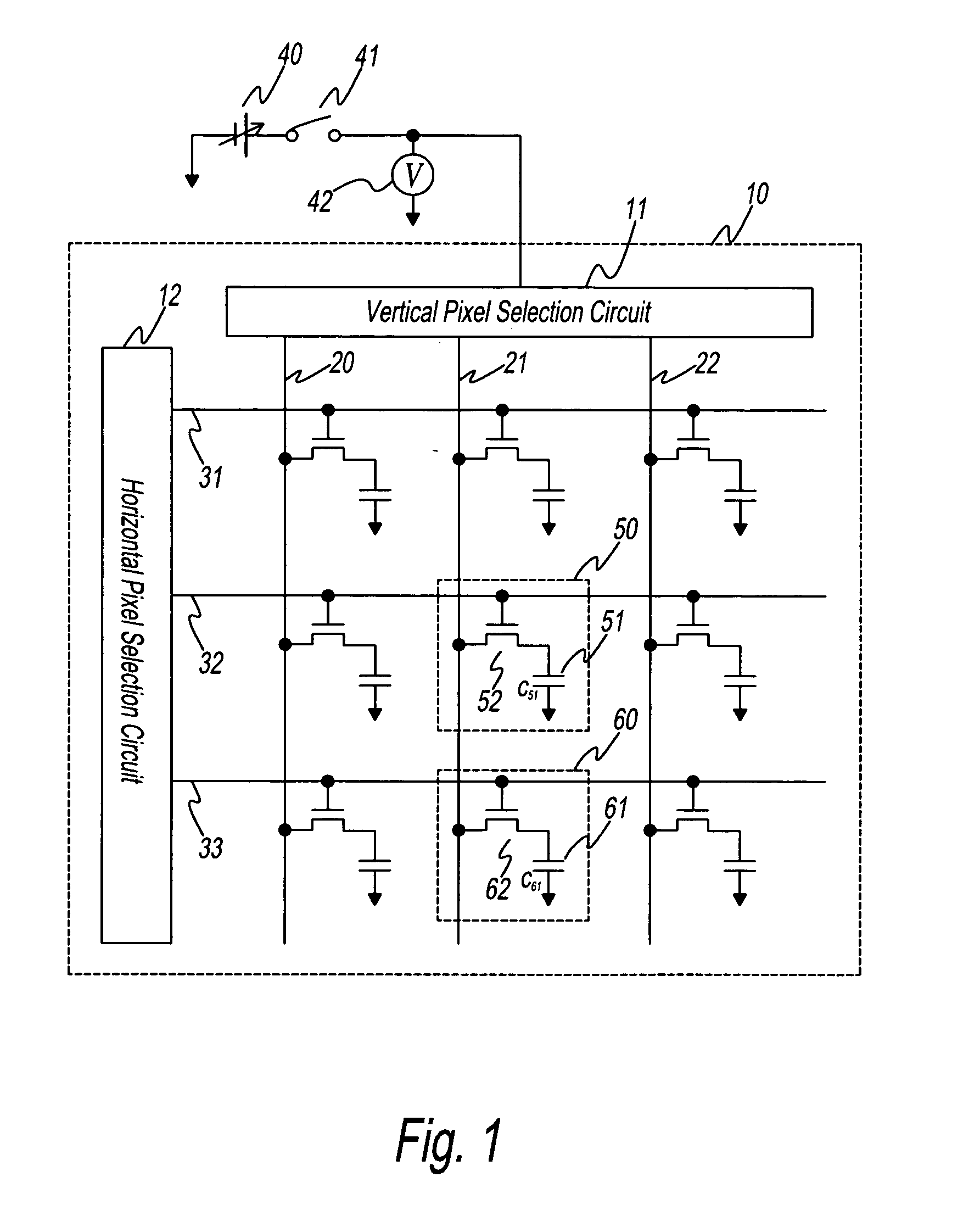
[0023]FIG. 1 shows the connection structure of the equipment of the method for testing related to the first embodiment according to the present invention. The TFT array 10 is identical to the one described in the Prior Art section. In the following description, to distinguish the capacitances, the capacitance of capacitor 51 is denoted by C51 and the capacitance of capacitor 61 is denoted by C61. When both capacitors 51, 61 are normal, the capacitances become equal (C51=C61). The voltmeter 42 and the switch 41 are connected to the input of the vertical pixel selection circuit 11, and a variable voltage source 40 is connected to the other terminal of the switch 41.

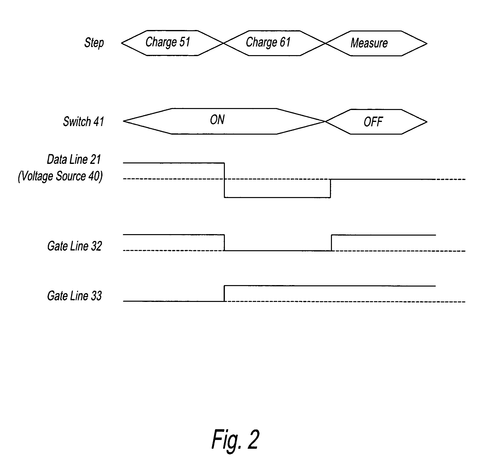
[0024] The method for testing related to the present invention is explained below based on the schematic drawing in FIG. 1 and the timing chart in FIG. 2. First, the voltage of the voltage source 40 is set to V1, and a gate line 32 is selected by the horizontal pixel selection circuit 12 and a data line 21 is selected by th...

second embodiment

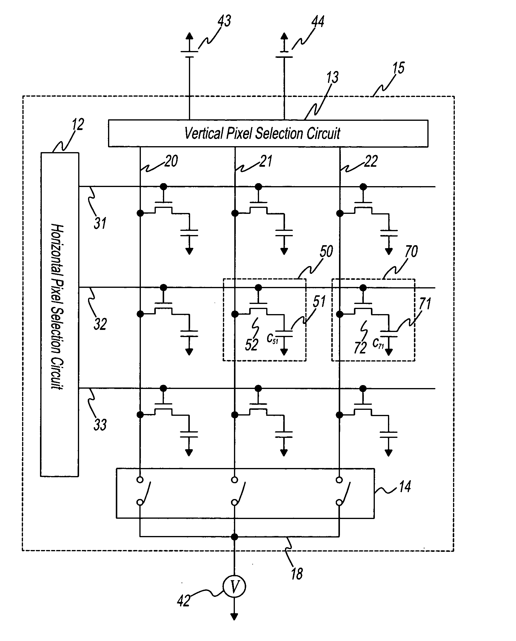
[0033] the present invention is explained with reference to the schematic drawing of FIG. 3 and the timing chart in FIG. 4. The TFT array 15 of the present embodiment differs from the TFT array 10 of the embodiment described previously in the function of the vertical pixel selection circuit 13 and the provision of switches 14. First, the vertical pixel selection circuit 13 has two input lines and a function for outputting the input signal from each input line to any data line. In addition, a switch 14 is provided at the terminal of each data line 20, 21, 22. A shared line 18 is set up at the other terminals of the switches 14, and all of the data lines can be electrically connected via the shared line 18 by setting the switches 14 in the “on” state.

[0034] In the test of the TFT array 15, voltage sources 43, 44 (output voltages of V1 and −V1, respectively) having output voltages of equal absolute values and opposite polarities are connected to the input of the vertical pixel selectio...


PUM


Abstract

A method for testing a TFT array that comprises one or a plurality of first pixels including capacitors connected to one terminal of pixel selection switches, one or a plurality of second pixels including capacitors connected to one terminal of pixel selection switches, and data lines connected to the other terminals of the pixel selection switches of the first pixels and the other terminals of the pixel selection switches of the second pixels, wherein the method for testing comprises a step for charging the capacitors of the first pixels to a first voltage, a step for charging the capacitors of the second pixels to a second voltage, a step for turning on both the pixel selection switches of the first pixels and the pixel selection switches of the second pixels, and a step for measuring either one or both of the voltage of a data line or the charge flowing through the data line.

Description

1. FIELD OF THE INVENTION [0001] The present invention relates to a method for testing thin film transistors (TFTs), more particularly, to testing the quality of the pixels in the TFT array in a flat panel display (FPD). 2. DISCUSSION OF THE BACKGROUND ART [0002] Over the past few years, flat panel displays such as liquid crystal displays and electroluminescent (EL) displays have become the main trends in displays. This type of FPD is constructed by enclosing liquid crystal or EL elements, which are the elements used for display, in a TFT array that arranges a plurality of pixels in a matrix. [0003]FIG. 5 shows a TFT array 10 of a typical liquid crystal display. The TFT array 10 is constructed from a plurality of pixels (i.e., 50) arranged in a matrix, pixel selection lines (i.e., 20, 30) for selecting the display pixels, and pixel selection circuits 11, 12 for controlling the pixel selection lines. [0004] A pixel 50 is constructed from a switching transistor 52 (pixel selection swi...

Claims


Application Information

Patent Timeline
IPC IPC(8): G01R19/00G01R31/00G01R31/26G02F1/1368G09F9/00G09G3/00G09G3/20G09G3/30
CPCG09G3/006G09G2300/0809G09G3/20G01R31/00
Inventor ITAGAKI, NOBUTAKA
Owner AGILENT TECH INC
Why Eureka
Try Eureka