Etch solution for selectively removing silicon and methods of selectively removing silicon

Active Publication Date: 2005-09-22
MICRON TECH INC
View PDF17 Cites 70 Cited by
  • Summary
  • Abstract
  • Description
  • Claims
  • Application Information

AI Technical Summary

Benefits of technology

[0012] While the specification concludes with claims particularly pointing out and distinctly claiming that which is regarded as the present invention, the advantage

Problems solved by technology

However, these etchants also aggressively etch other materials, such as metals, oxides, polyimides, or nitrides, which are commonly present on the substrate as portions of an integrated circuit being fabricated thereon.
Therefore, if the integrated circuit include

Method used


Image

  • Etch solution for selectively removing silicon and methods of selectively removing silicon
  • Etch solution for selectively removing silicon and methods of selectively removing silicon
  • Etch solution for selectively removing silicon and methods of selectively removing silicon

Examples


Example

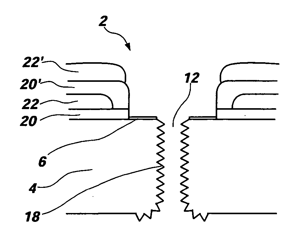
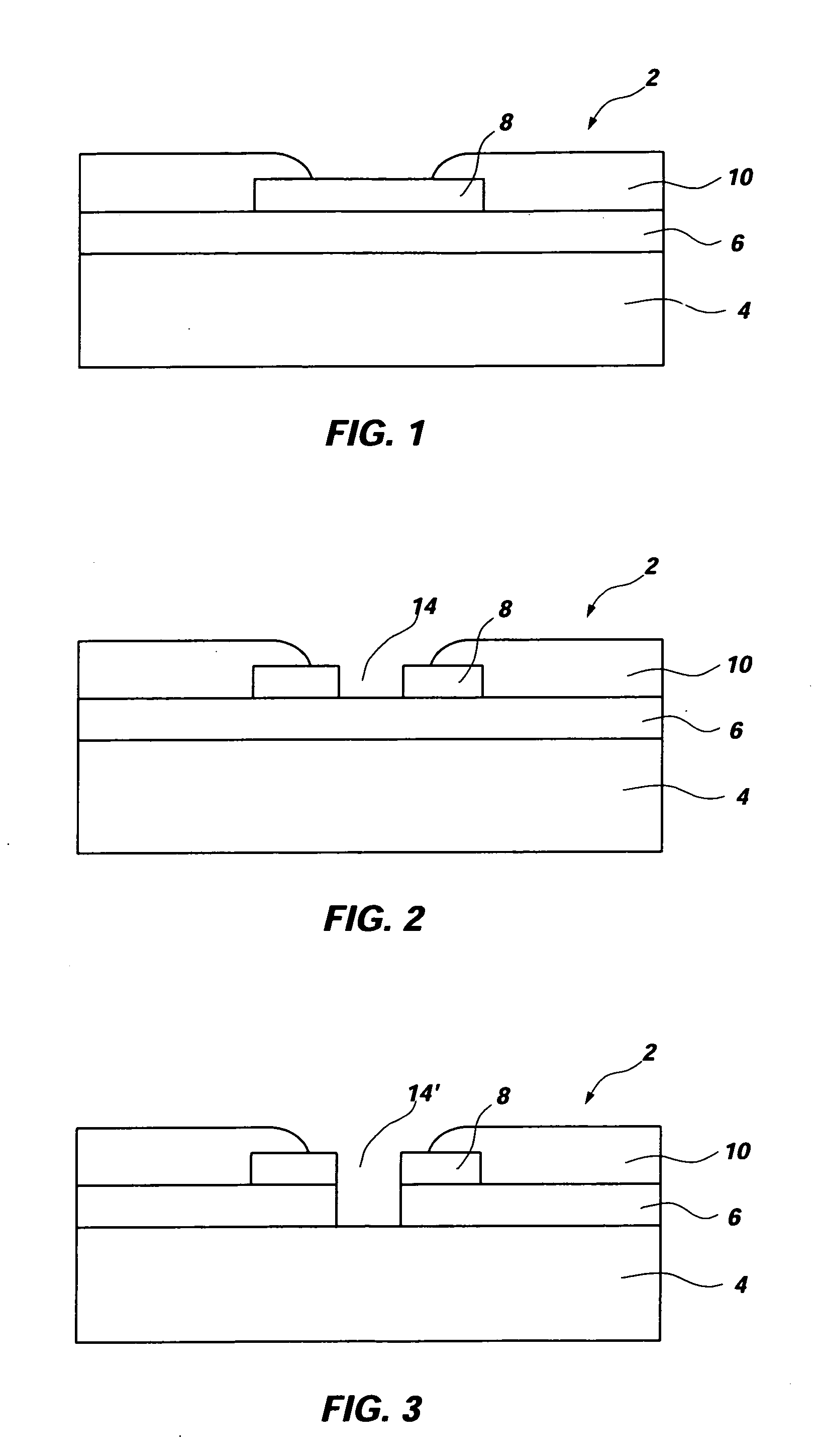
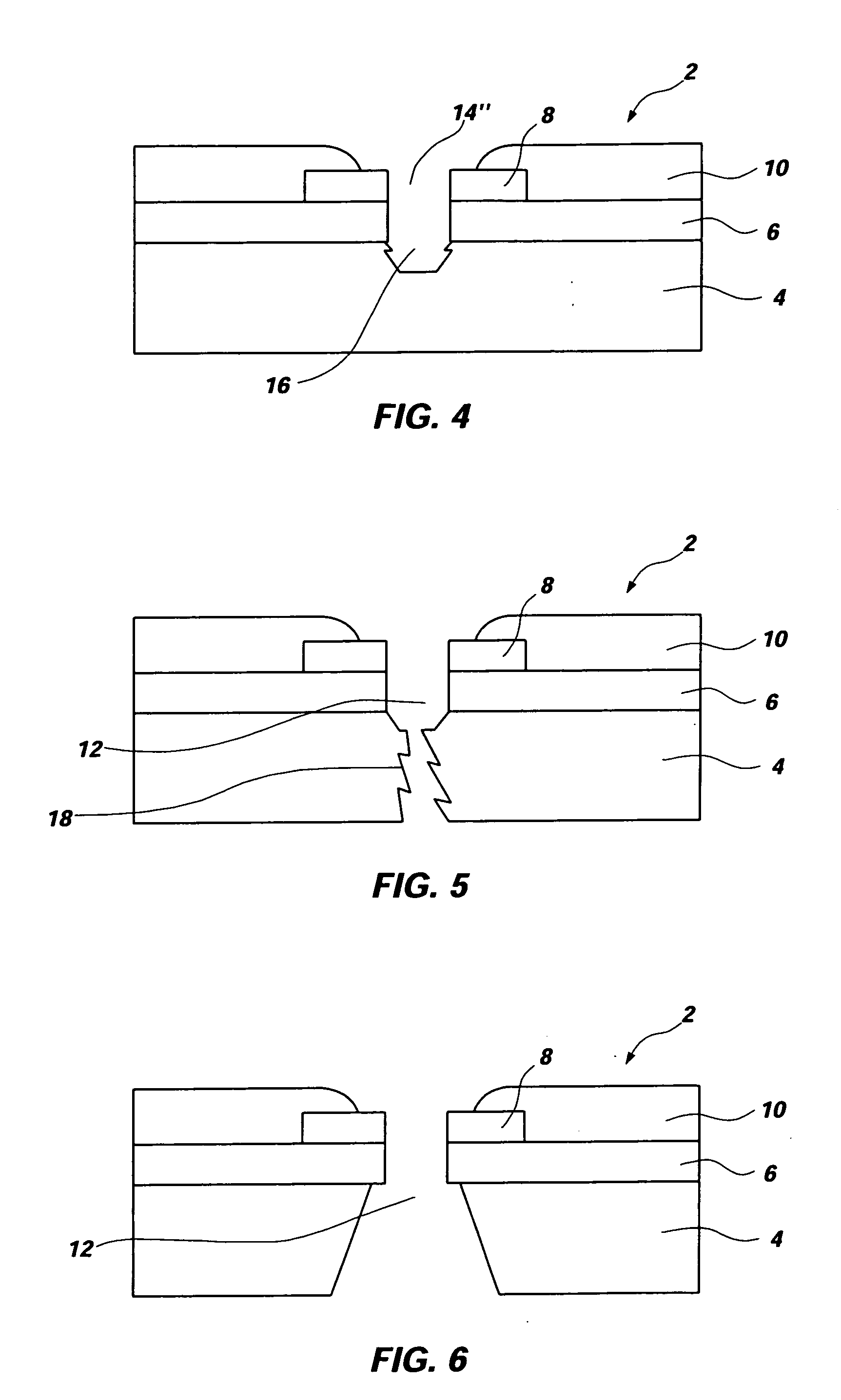
[0017] An etch solution that includes TMAH and at least one organic solvent is disclosed. The etch solution may be used to selectively etch or remove a silicon layer from a substrate without etching or removing other materials on the substrate. As used herein, the term “silicon layer” refers to a layer or feature formed from silicon including, but not limited to, monocrystalline silicon or polycrystalline silicon (“polysilicon”). The etch solution may selectively etch the silicon layer without removing or etching other layers or features on the substrate, such as metal, oxide, polyimide, or nitride layers. Instead of TMAH, the etch solution may also utilize additional tetraalkylammonium hydroxides including, but not limited to, tetraethylammonium hydroxide. In addition, mixtures of tetraalkylammonium hydroxides may be used, such as mixtures of tetraethylammonium hydroxide and TMAH. The etch solution may etch the silicon layer at a rate that is commercially viable for removing the si...


PUM


Abstract

An etch solution that comprises tetramethylammonium hydroxide (“TMAH”) and at least one organic solvent. The etch solution may be substantially free of water. The etch solution is formulated to selectively etch a silicon layer relative to other layers on an integrated circuit. The TMAH may be present in an amount ranging from approximately 1% by weight to approximately 10% by weight. The at least one organic solvent may be selected from the group consisting of isopropanol, butanol, hexanol, phenol, glycol, glycerol, ethylene glycol, propylene glycol, glycerin, and mixtures thereof. A method of selectively etching a silicon layer and a method of removing a heat-affected zone (“HAZ”) on an integrated circuit are also disclosed.

Description

FIELD OF THE INVENTION [0001] The present invention relates to a composition and method of etching silicon and, more specifically, relates to a composition and method of selectively etching silicon without etching metal, oxide, or nitride materials. BACKGROUND OF THE INVENTION [0002] Semiconductor devices, from microprocessors to memory chips, are fabricated by performing a complex series of processes that include depositing various materials and selectively masking and etching one or more materials on portions of a semiconductor wafer or other bulk semiconductor substrate. Silicon is a conductive material that is commonly used as a semiconductor substrate in a semiconductor device, such as in an integrated circuit. Ideally, etching selectively removes or etches portions of the semiconductor substrate without damaging or removing other portions. In a wet etch process, a wet etch solution is typically applied to a surface of the semiconductor substrate. Reactants in the wet etch solu...

Claims


Application Information

Patent Timeline
IPC IPC(8): H01L21/302H01L21/306H01L21/461
CPCH01L21/30608
Inventor KIRBY, KYLE K.TOREK, KEVIN J.
Owner MICRON TECH INC
Why Eureka
Try Eureka