Fingerprint sensing pixel with a larger aperture

a fingerprint sensing pixel and aperture technology, applied in the field of fingerprinting touch screen panels, can solve the problems of dimmer fingerprinting area on the lcd display screen region of the fingerprinting touch screen panel region of the lcd display system, and may not be optimal for some applications for aesthetic reasons

Inactive Publication Date: 2005-10-06
AU OPTRONICS CORP
View PDF14 Cites 110 Cited by
  • Summary
  • Abstract
  • Description
  • Claims
  • Application Information

AI Technical Summary

Benefits of technology

[0008] According to another embodiment of the present invention, a thin film transistor-based resistive-type fingerprinting touch screen panel is also disclosed. The touch screen panel comprises an upper substrate and a lower substrate positioned beneath the upper substrate. The upper substrate is usually a flexible PET film having a conductive coating layer on the underside. The lower substrate comprises an array of thin film transistor-based sensing pixels. Each of the sensing pixels comprises a thin film transistor having a poly-Si film layer forming a channel region and at least one drain electrode connecting the poly-Si film layer to a contact metal pad. A sensing electrode of the pixel is connected to the contact metal pad through a via, wherein at least a portion of the via overlaps the poly-Si film layer when viewed through the sensing electrode. The sensing electrode may be made of a transparent material such as indium tin oxide or indium zinc oxide.

Problems solved by technology

This results in the fingerprinting touch screen panel region of the LCD display system to appear dimmer than the rest of the LCD display area.
Although this has no effect on the functional aspects of the fingerprinting touch screen panel or the LCD display, having a dimmer fingerprinting area on the LCD display screen may not be optimal for some applications for aesthetical reasons.

Method used


Image

  • Fingerprint sensing pixel with a larger aperture
  • Fingerprint sensing pixel with a larger aperture
  • Fingerprint sensing pixel with a larger aperture

Examples


Embodiment Construction

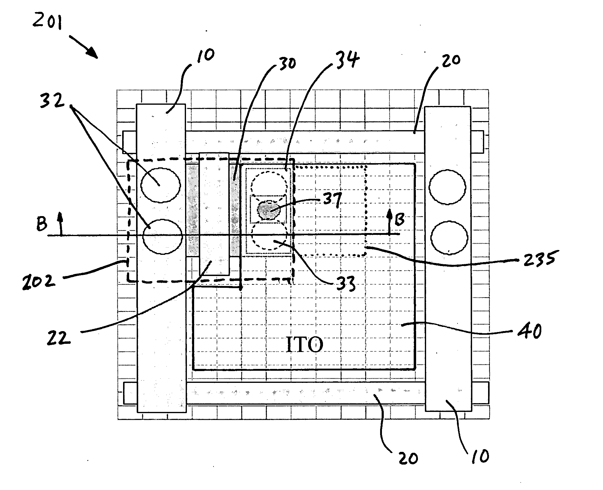
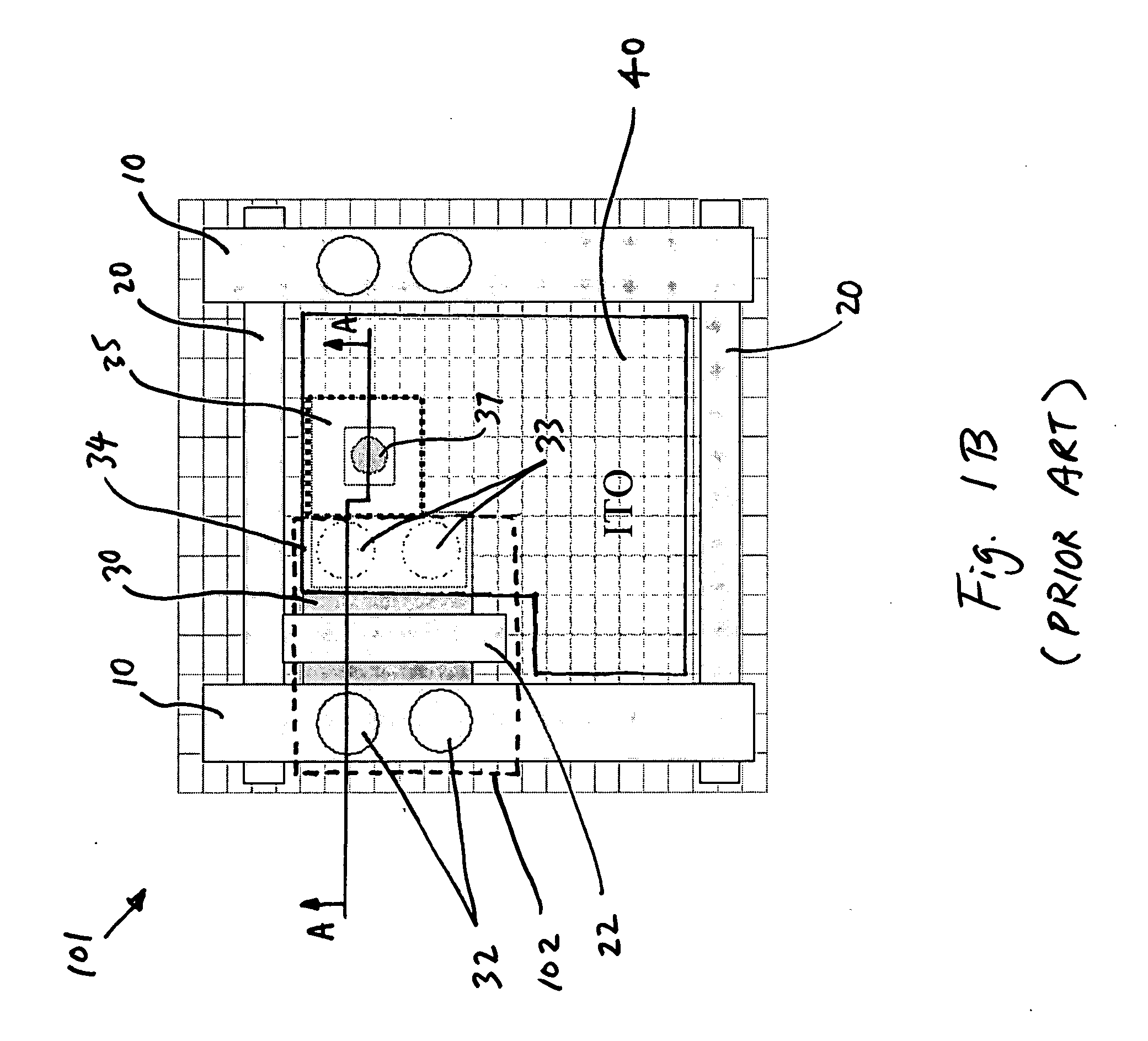
[0016]FIG. 2A illustrates a plan view of a pixel region 201 of an improved fingerprinting touch screen panel according to an embodiment of the present invention. Comparing this improved structure to the pixel region 101 of the conventional fingerprinting touch screen panel 100 of FIG. 1C, the extended portion 35 of the drain contact metal pad 34 has been removed. This is represented by a phantom line 235 showing the outline of where the extended portion 35 would be in a conventional fingerprinting touch screen panel. Thus, in the improved fingerprinting touch screen panel according to an aspect of the present invention, the total area of opaque metalized portion in the pixel region 201 has been reduced. In turn, the transparent region is larger and the aperture ratio of the pixel region 201 is higher than the aperture ration of the pixel region 101, for example, of the conventional fingerprinting touch screen panel 100.

[0017] To achieve this improvement, the via 37 connecting the I...


PUM

PropertyMeasurementUnit
transparentaaaaaaaaaa
flexibleaaaaaaaaaa
transparent conductiveaaaaaaaaaa

Abstract

In a thin film transistor-based resistive-type fingerprinting touch screen panel, the size of the contact metal layer connecting the drain electrode of the TFT and the ITO sensing electrode in each of the pixel regions of the touch screen panel is reduced, thus increasing the aperture of the pixel region. Having a greater aperture, more of the backlighting from the LCD display panel usually positioned behind the touch screen panel is transmitted through the touch screen panel, making that region brighter.

Description

FIELD OF THE INVENTION [0001] The present invention relates to fingerprinting touch screen panels and more particularly to fingerprinting touch screen panels having high aperture ratio to allow more backlighting to transmit through the touch screen panels. BACKGROUND OF THE INVENTION [0002] Touch screen panels are commonly used in combination with liquid crystal display (LCD) devices. In many such applications, the touch screen panels function as contact switches to allow graphically rendered buttons and switches on the LCD screen to function as if they are real buttons and switches. More recent development in the touch screen panel technology has produced touch screen panels for acquiring fingerprint images directly on the touch screen panels. A general description of an example of such fingerprinting touch screen panel is illustrated in FIGS. 1A-1C. [0003]FIG. 1A is a cross-sectional view of a thin film transistor-based resistive-type touch screen panel 100 for acquiring fingerpri...

Claims


Application Information

Patent Timeline
Patent Type & Authority Applications(United States)
IPC IPC(8): G02F1/133G06F3/033G09G5/00
CPCG02F1/13338G06F2203/0338G06F3/03547
Inventor WENG, CHIEN-SEN
Owner AU OPTRONICS CORP
Why Eureka
Try Eureka