
System for providing an integrated circuit with a unique identification

a technology of integrated circuits and unique identification, applied in the direction of individual semiconductor device testing, noise figure or signal-to-noise ratio measurement, instruments, etc., can solve the problems of adding cost and time to the manufacturing process, adding additional processing steps needed to customize each individual chip,

Inactive Publication Date: 2000-12-12
ICID
View PDF16 Cites 326 Cited by
  • Summary
  • Abstract
  • Description
  • Claims
  • Application Information

AI Technical Summary

Benefits of technology

The ICID circuit of the present invention provides a means for enabling each of millions of chips to uniquely and reliably identify itself without having to customize each individual chip using costly and time-consuming additional processing steps during or after chip fabrication.
The concluding portion of this specification particularly points out and distinctly claims the subject matter of the present invention. However, those skilled in the art will best understand both the organization and method of operation of the invention, together with further advantages and objects thereof, by reading the following descriptions in view of the accompanying drawings wherein like reference characters refer to like elements.

Problems solved by technology

These methods of identification are useful for indicating the type of component being manufactured or placed in an assembly, but they do not distinguish individual chip one from another.
While such approaches are effective to provide each chip with an ID, the additional processing steps needed to customize each individual chip add time and cost to the chip manufacturing process.
While such methods can provide each chip with a unique identification, they require special processing steps during the semiconductor manufacturing process that add cost and time to the manufacturing process.

Method used


Image

  • System for providing an integrated circuit with a unique identification
  • System for providing an integrated circuit with a unique identification
  • System for providing an integrated circuit with a unique identification

Examples


Embodiment Construction

)

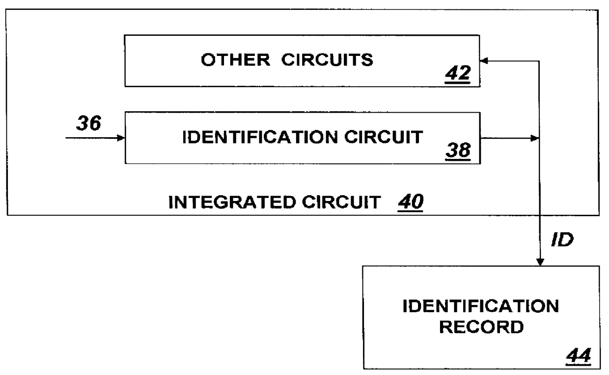
The present invention relates to an integrated circuit identification (ICID) circuit 38 as illustrated in FIG. 1 that may be incorporated into an integrated circuit (IC) chip 40 along with other circuits 42. In response to control and timing data arriving via control inputs 36, ICID 38 generates an output data sequence (ID) at IC output terminal ID that uniquely identifies IC chip 40. After fabricating IC chip 40, a manufacturer may record the output ID of ICID circuit 38 in an identification record 44. Thereafter that particular chip 40 can be identified whenever and wherever that chip may be found by the unique ID produced by its ICID 38 when control inputs 36 signal it to do so.

It has been known to provide each of a large number of IC chips with a non-volatile memory for storing and reading out an ID uniquely identifying each chip. However such prior art chip ID systems require that a separate ID be written into each individual IC using additional processing steps during or afte...


PUM


Abstract

An integrated circuit identification device (ICID) to be incorporated into an integrated circuit (IC) includes an array of electronic cells in which the magnitude of an output signal of each cell is a function of randomly occurring parametric variations which vary from cell-to-cell. The ICID also includes a circuit for measuring the output of each cell and for producing output data having a value reflecting the particular combination of measured characteristics of all of the elements of the array. When we make the number of elements in the array large enough, we insure that to a high degree of probability, the pattern of measured array cell characteristics for an ICID embedded in any one IC will be unique and distinguishable from such patterns measured by ICIDs embedded in millions of other ICs. Thus the value of the output data produced by an ICID circuit acts as a unique "fingerprint" for the IC in which it is installed, and can be used as a unique identification (ID) for that IC.

Description

1. Field of the InventionThe present invention relates in general to a system for uniquely identifying an integrated circuit (IC), and in particular to a device that may be embedded in the IC which, due to randomly occurring chip-to-chip or device-to-device parametric variations, produces a unique output identification for each IC chip in which it is implemented.2. Description of Related ArtIntegrated circuits are manufactured with batch processing intended to make all integrated circuit chips identical, thereby lowering manufacturing costs and improving quality. However, it is useful to be able to distinguish each individual integrated circuit from all others, for example to track its source of manufacture, or to identify a system employing the integrated circuit. Individually identifiable integrated circuits can be used to validate transactions, route messages, track items through customs, verify royalty counts, recover stolen goods, validate software, and many other uses.It has b...

Claims


Application Information

Patent Timeline
IPC IPC(8): H01L23/544
CPCH01L23/544H04L9/0866H01L2223/54433H01L2223/5444H01L2223/54473H01L2924/3011H01L2924/0002H01L2924/00
Inventor LOFSTROM, KEITH
Owner ICID
Learn More