

Manufacturing method of nitride semiconductor device and nitride semiconductor device
- Summary
- Abstract
- Description
- Claims
- Application Information
AI Technical Summary
Benefits of technology
Problems solved by technology
Method used
Image

Examples
first embodiment
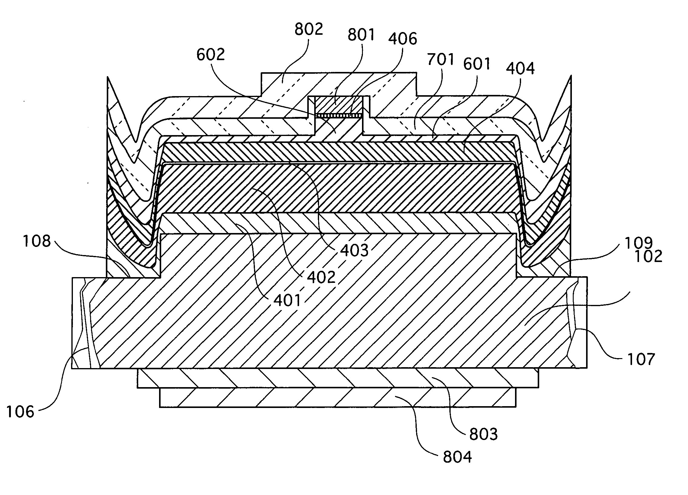
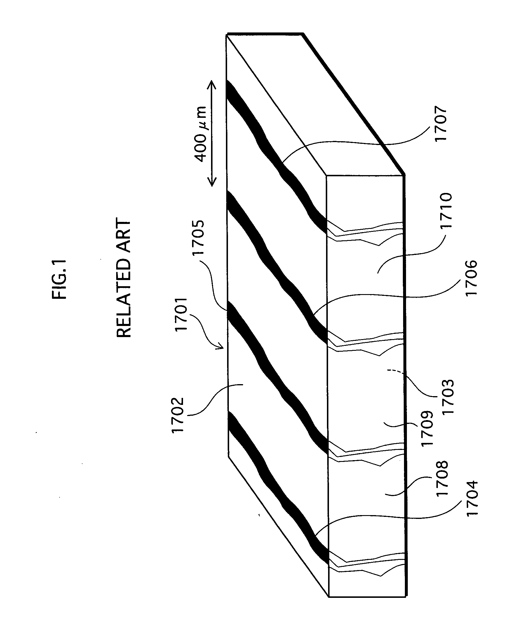
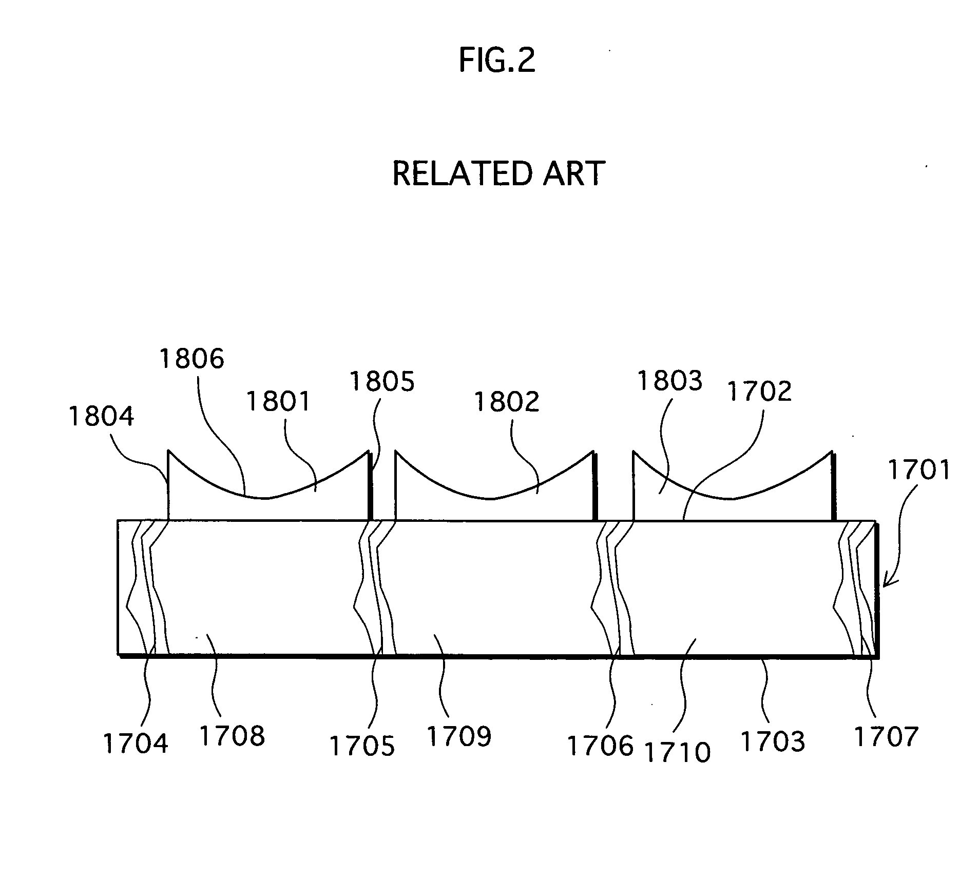
[0053]FIG. 3 is a sectional diagram drawn to explain film thickness of a layer structure formed on a GaN substrate in a nitride semiconductor device according to the first embodiment of the present invention.
[0054] In a nitride semiconductor device 101, a layer structure, which is made of a crystal growth layer 104 of a nitride semiconductor, is formed on a front surface 103 of a GaN substrate 102.
[0055] In the GaN substrate 102, dislocation concentrated regions 106 and 107 are formed. The dislocation concentrated regions 106 and 107 have concentrated therein defect crystals and align as stripes that pass through the GaN substrate 102 from the front surface 103 to a back surface 105. Moreover, grooves 108 and 109 are formed along a direction in which the dislocation concentrated regions 106 and 107 extend.
[0056] Then, crystal growth materials including group-III element and N element (e.g. Ga, Al, In) are supplied, using the MOCVD method, to the front surface 103 of the GaN subst...
PUM
 Abstract
Description
Claims
Application Information