Device-level address translation within a programmable non-volatile memory device

a technology of non-volatile memory and device level, applied in the direction of memory adressing/allocation/relocation, instruments, computing, etc., can solve the problems of flash translation layer, inability to achieve translation between logical and physical addresses, and relatively complex software that consumes valuable resources

Active Publication Date: 2005-10-06
RIVERSTONE NETWORKS +1
View PDF6 Cites 21 Cited by
  • Summary
  • Abstract
  • Description
  • Claims
  • Application Information

AI Technical Summary

Problems solved by technology

Because the flash translation layer is an entirely software-based element, when the operating system and flash translation layer are not up and running, no translation between logical and physical addresses can be accomplished.
While the flash translation layer works well to provide software-level address translation between an operating system and a flash memory device, the flash translation layer is relatively complex software that consumes valuable resources (RAM memory space, processing cycles) in a computer system.

Method used


Image

  • Device-level address translation within a programmable non-volatile memory device
  • Device-level address translation within a programmable non-volatile memory device
  • Device-level address translation within a programmable non-volatile memory device

Examples


Embodiment Construction

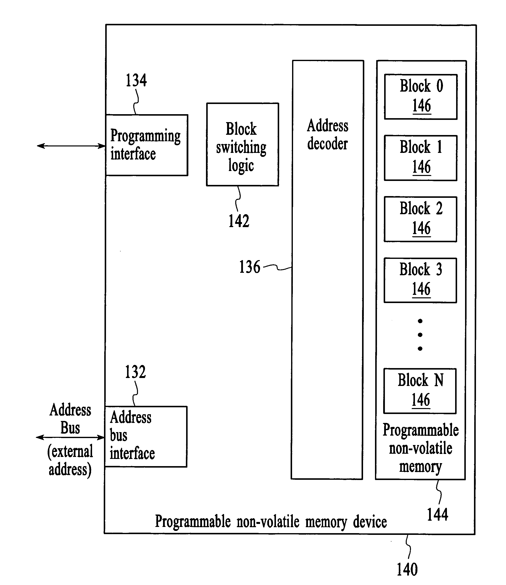
[0026]FIG. 4 depicts a block diagram of a computer system 130 that includes a processor 132 and a programmable non-volatile memory device 140. The processor can be any type of processor from a simple single function processor to a multifunction central processing unit. The programmable non-volatile memory device may be any programmable non-volatile memory device including, for example, a flash memory device, EEPROM, non-volatile RAM, a complex programmable logic device (CPLD), flash-based field programmable gate arrays (FPGAs), and battery-backed RAM. The processor communicates addresses to the programmable non-volatile memory device to control read and write operations. The addresses that are received by the programmable non-volatile memory device are referred to herein as “external addresses” because the addresses are received from an element that is external to the programmable non-volatile memory device.

[0027] In accordance with an embodiment of the invention, the programmable ...


PUM


Abstract

A programmable non-volatile memory device includes block switching logic that enables device-level translation rules to be changed. The device-level translation rules map the external addresses received by the flash memory device to the internal addresses of the programmable non-volatile memory device. Because the device-level translation rules are changeable, the physical location in the programmable non-volatile memory device to which an external address maps can be changed in a manner that is transparent to off-device operations. By allowing device-level translation rules to be changed, block management functions can be accomplished within the programmable non-volatile memory device itself.

Description

CROSS REFERENCE TO RELATED APPLICATIONS [0001] This application is entitled to the benefit of provisional U.S. Patent Application Ser. No. 60 / 556,283, filed 25 Mar. 2004.FIELD OF THE INVENTION [0002] The invention relates generally to programmable non-volatile memory devices, and more particularly, to techniques for managing data reads and writes within a programmable non-volatile memory device. BACKGROUND OF THE INVENTION [0003] Programmable non-volatile memory such as flash memory and electronically erasable programmable read only memory (EEPROM) is used in many types of computer systems. For example, programmable non-volatile memory is used in computer systems where space is a premium (e.g., mobile phones, PDAs, digital cameras) and in computer systems where high-reliability is critical (e.g., communications network equipment). A common use of programmable non-volatile memory is to store a boot program for a processor. Programmable non-volatile memory can also be used to store da...

Claims


Application Information

Patent Timeline
Patent Type & Authority Applications(United States)
IPC IPC(8): G06F12/02G06F12/08
CPCG06F12/0246G06F12/0292
Inventor BELEVICH, ARTEMBALAKRISHNAN, THIRUMALPATHY
Owner RIVERSTONE NETWORKS
Why Eureka
Try Eureka