Plasma display device and method of driving the same

a technology of display device and display device, which is applied in the direction of static indicating device, identification means, instruments, etc., can solve the problems of reducing the contrast ratio, lowering reducing the contrast value of the dark room, so as to improve the operational margin and increase the contrast of the dark room

Inactive Publication Date: 2005-10-13
LG ELECTRONICS INC
View PDF9 Cites 24 Cited by
  • Summary
  • Abstract
  • Description
  • Claims
  • Application Information

AI Technical Summary

Benefits of technology

[0038] Accordingly, the present invention has been made in view of the above problems occurring in the prior art, and it is an object of the present invention to provide a plasma display...

Problems solved by technology

Thus, there are problems in that a dark room contrast value is lowered and the contrast ratio is thus lowered.
This causes the dark room contrast value to drop.
If the dark discharge is insufficient during the set-up period SU, the condition within the discharge cell immediately after the reset period fails to result in an optimal address condition.
Therefore, abnormal discharge or erroneous discharge will occur.
Initialization is therefore not uniform in each of the cells throughout the entire display.
That is, if the discharge during the erase period is strong (i.e., before the reset period), erroneous discharge can occur.
However, although these wall charges must be erased so that initialization is normally performed in a next sub-field, the polarity of the wall charges remains intact if the erase discharge is not generated or the erase discharge is very weak.
Resultantly, if the erase discharge is not generated or the erase discharge is very weak in the erase period before the reset period, erroneous discharge or abnormal discharge occurs since initialization is not performed in a normal manner.
As a result, if the initial gap voltage Vgini ...

Method used


Image

  • Plasma display device and method of driving the same
  • Plasma display device and method of driving the same
  • Plasma display device and method of driving the same

Examples


first embodiment

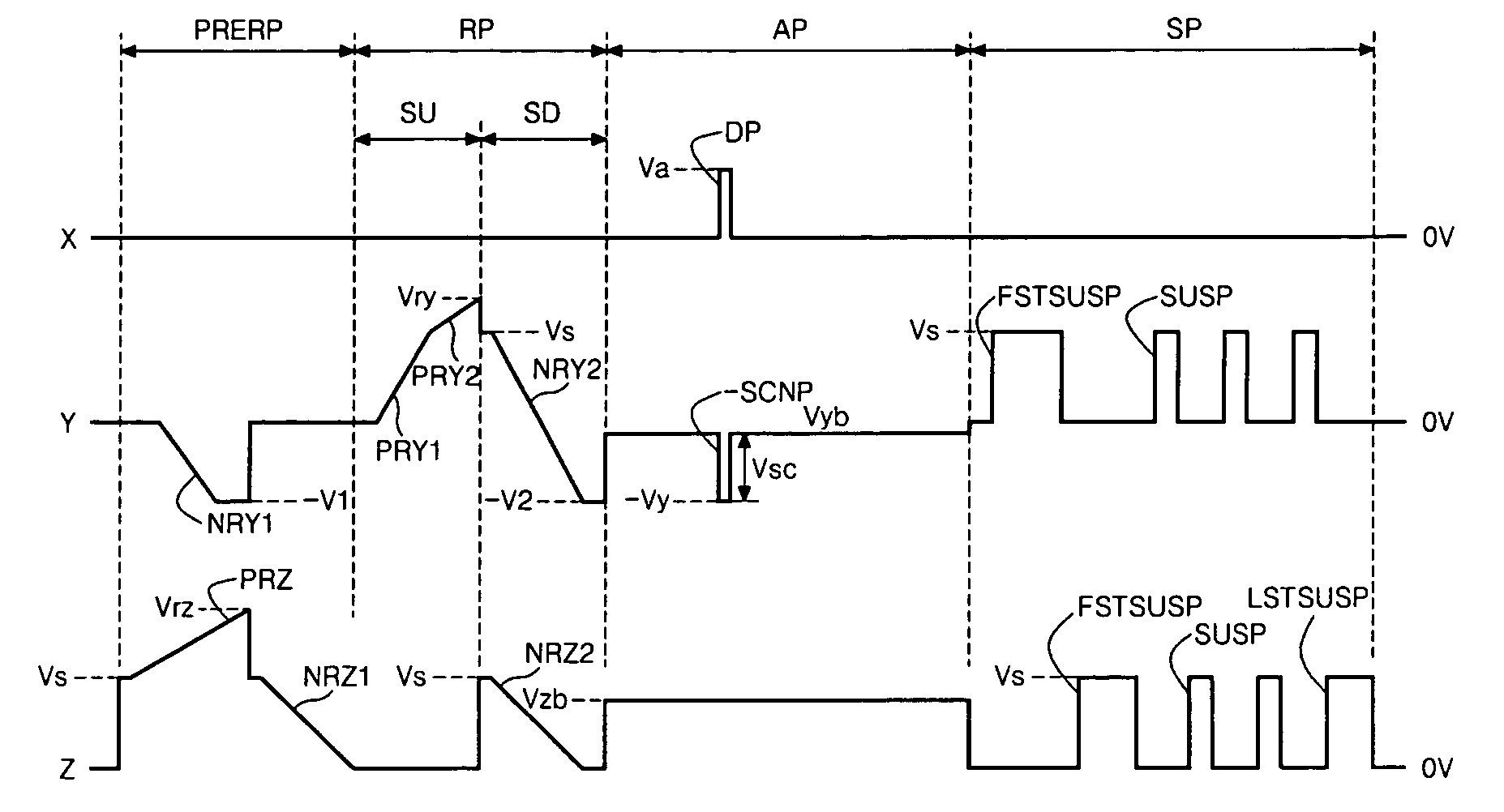
[0076]FIG. 6 shows a driving waveform supplied to the PDP shown in FIG. 2 during a first sub-field period, for driving a PDP according to the present invention. The driving waveform of FIG. 6 will be described in conjunction with the distribution of wall charges shown in FIGS. 7a to 7e.

[0077] Referring to FIG. 6, in one method of driving the PDP according to the present invention, a first sub-field includes a pre-reset period PRERP for forming wall charges of the positive polarity on the scan electrodes Y and wall charges of the negative polarity on the sustain electrodes Z, a reset period for initializing discharge cells of the entire screen using wall charge distribution established during the pre-reset period PRERP, an address period AP for selecting discharge cells, and a sustain period SP for sustaining discharging of selected discharge cells. In the present embodiment, as shown in FIG. 7a, positive electric charges at the scan electrodes sufficiently accumulate by means of su...

second embodiment

[0105]FIG. 14 shows a waveform for explaining a method of driving a plasma display apparatus according to the present invention.

[0106]FIG. 14 illustrates a waveform for use in a method of driving the plasma display apparatus according to a second embodiment of the present invention. In this embodiment, the second Z negative ramp waveform NRZ2 reaches the reference voltage GND before the second Y negative ramp waveform NRY2 reaches the reference voltage GND.

[0107] In the present embodiment, the pre-reset period PRERP, the set-up period SU of the reset period RP, the address period AP and the sustain period SP are substantially the same as those of the aforementioned embodiment. A detailed description thereof will be thus omitted for simplicity.

[0108] During the set-down period SD of the reset period RP, the second Z negative ramp waveform NRZ2 is applied to the sustain electrodes Z simultaneously when the second Y negative ramp waveform NRY2 is applied to the scan electrodes Y. The...

third embodiment

[0109]FIG. 15 shows a driving waveform of a first sub-field in a method of driving a plasma display apparatus according to the present invention. As shown, during a pre-reset period PRERP, a ramp waveform is not supplied to sustain electrodes Z, instead, a sustain voltage in the form of a square type wave is supplied to the sustain electrodes Z, so that negative wall charges accumulate on the sustain electrodes Z. During a set-down period SD, a square type wave is supplied to the sustain electrodes Z, so that the sustain electrodes Z are maintained at a positive bias voltage. It will be understood that a square type wave is one in which the voltage changes from approximately 10 percent to 90 percent of its maximum value over a time period that is generally less than 10 μs, remains substantially level for a second period of time, and then changes from 90 percent to 10 percent of its maximum value over yet a third period of time that is, once again, generally less than 10 μs.

[0110] In...


PUM


Abstract

The present invention relates to a plasma display apparatus and method of driving the same, wherein erroneous discharge, miss-discharge and abnormal discharge are prevented, dark room contrast is increased, and operational margin is widened. According to the plasma display apparatus and driving method thereof, a negative voltage is applied to a first electrode, and a positive voltage is applied to a second electrode, whereby wall charges of a positive polarity are accumulated on the first electrode and wall charges of a negative polarity are accumulated on the second electrode, within discharge cells during a pre-reset period. The discharge cells are then initialized using the wall charge distribution of the discharge cells during a reset period.

Description

CROSS-REFERENCES TO RELATED APPLICATIONS [0001] This Nonprovisional application claims priority under 35 U.S.C. § 119(a) on Patent Application No. 10-2004-0022816 filed in Korea on Apr. 2, 2004, Patent Application No. 10-2004-0095452 filed in Korea on Nov. 19, 2004, and Patent Application No. 10-2004-0092135 filed in Korea on Nov. 11, 2004, and Patent Application No. 10-2005-0018887 filed in Korea on Mar. 7, 2005, the entire contents of which are hereby incorporated by reference. BACKGROUND OF THE INVENTION [0002] 1. Field of the Invention [0003] The present invention relates to a plasma display apparatus, and more particularly, to a plasma display apparatus and method of driving the same, wherein erroneous discharge, miss-discharge and abnormal discharge are prevented, dark room contrast is increased, and operational margin widens. [0004] 2. Background of the Related Art [0005] A plasma display panel (hereinafter, referred to as “PDP”) is adapted to display an image by light-emitti...

Claims


Application Information

Patent Timeline
IPC IPC(8): G09F9/313G09G3/20G09G3/288G09G3/291G09G3/292G09G3/293G09G3/294G09G3/298H01J17/49
CPCG09G3/2022G09G3/2922G09G3/2927G09G3/294G09G2320/041G09G2310/066G09G2320/0228G09G2320/0238G09G3/2948
Inventor JUNG, YUN KWONYANG, HEE CHANSEO, JU WONKANG, BONG KOOKIM, JIN YOUNG
Owner LG ELECTRONICS INC
Why Eureka
Try Eureka