Method for improved high current component interconnections

a high-current component and interconnection technology, applied in the field of forming solder interconnections, can solve the problems of excessive parasitic inductance, and limit the effectiveness of the power delivery system

Inactive Publication Date: 2005-10-13
AMIR DUDI I +1
View PDF7 Cites 3 Cited by
  • Summary
  • Abstract
  • Description
  • Claims
  • Application Information

AI Technical Summary

Problems solved by technology

One potential power delivery bottleneck is in the printed circuit board-component interface.
For example, a power MOSFET-board interface can introduce a substantial amount series resistance and thereby limit the effectiveness of the power delivery system.
These smaller interconnects are highly resistive, and can limit the effectiveness of the power delivery system.
In addition, the resulting high current density can result in excessive parasitic inductance.
This may not provide for an optimal solder interconnection, however.
Solder voids 124 and solder separation will result from insufficient solder volume.
However, this requires a change in product design by the component vendor to accommodate the additional solder on the component package.
Because of limitations on the amount of solder paste that can practically be applied to the printed circuit board, the solder paste alone provides insufficient solder volume to entirely fill the solder interconnections 123.

Method used


Image

  • Method for improved high current component interconnections
  • Method for improved high current component interconnections
  • Method for improved high current component interconnections

Examples


Embodiment Construction

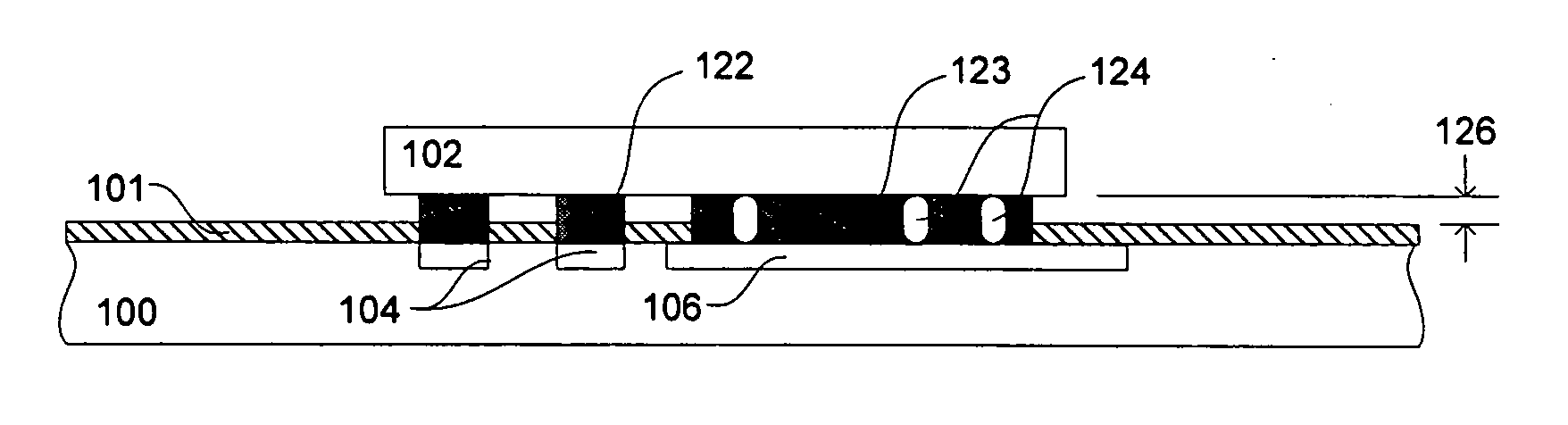
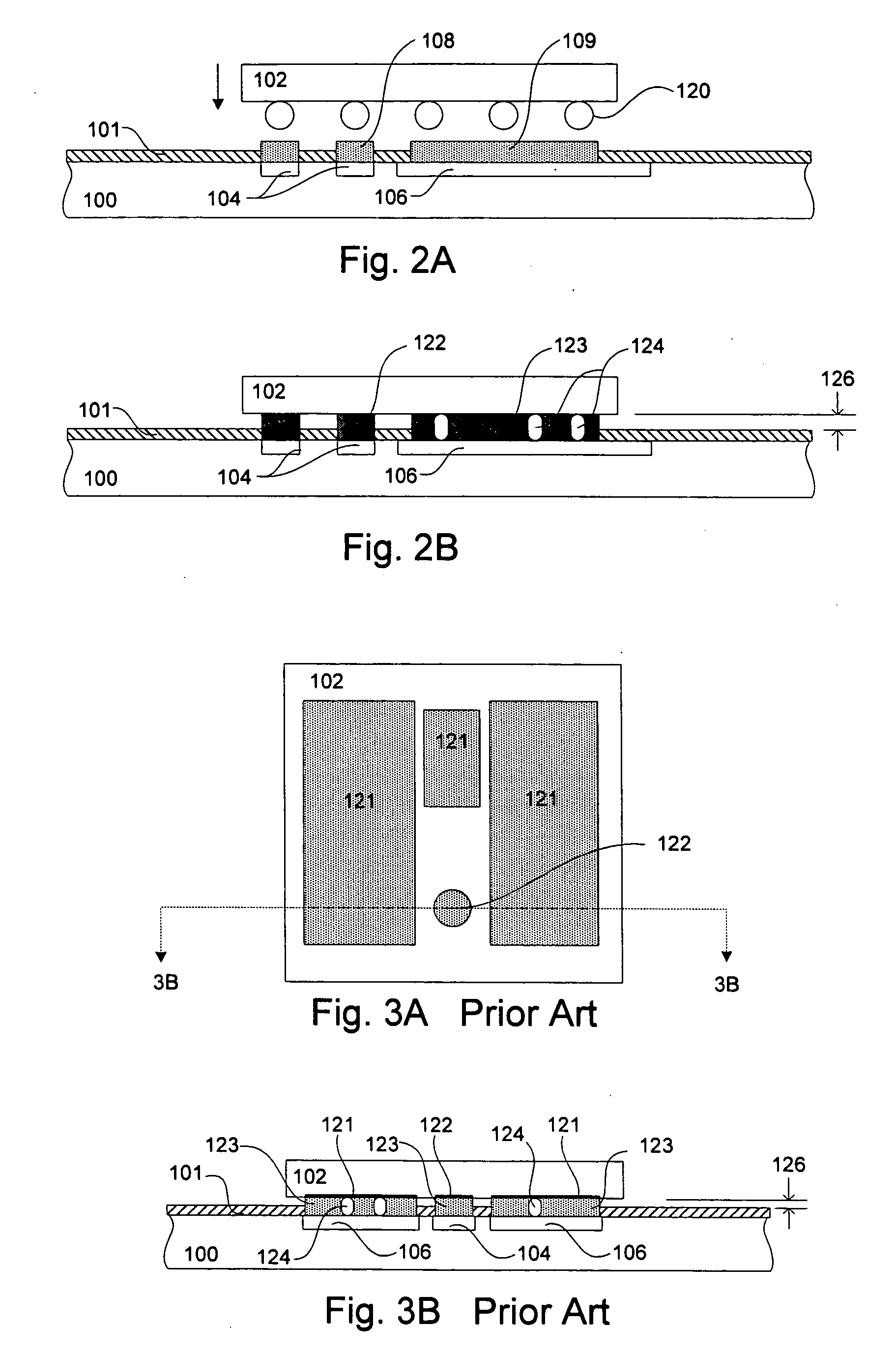
[0031] Embodiments of the present invention provide a method for widening the power delivery interface between the printed circuit board and the component through printed circuit board manufacturing processes alone, and without requiring a re-design of existing components. This is accomplished by placing pre-formed solder elements in selected areas of solder paste where additional solder volume is required.

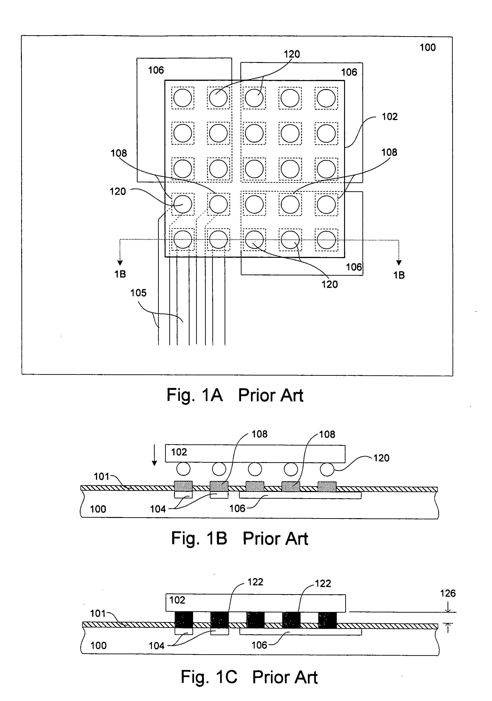
[0032]FIG. 4A illustrates a top view of a printed circuit board 300 prior to application of solder paste. A solder paste stencil 303 containing apertures 307 is placed over the printed circuit board. The solder paste stencil is positioned over the printed circuit board such that the apertures 307 in the stencil correspond to areas on the printed circuit board where solder paste application is desired. The location of the apertures in the solder paste stencil corresponds to areas on the printed circuit board where there will be an electrical connection to a component. The aperture...


PUM


Abstract

A printed circuit board having at least one conductive region covered in solder paste has preformed solder elements placed on the solder paste in the conductive region. A component package is placed onto the printed circuit board over the conductive region and the solder is reflowed, forming a wide solder interconnection between the component and the conductive region of the printed circuit board.

Description

[0001] This is a Divisional application Ser. No. 10 / 427,681 filed Apr. 30, 2003, which is presently pending.BACKGROUND OF THE INVENTION [0002] 1. FIELD OF THE INVENTION [0003] The present invention relates generally to the field of electronic printed circuit boards, and more specifically to forming solder interconnections on the printed circuit board. [0004] 2. DISCUSSION OF RELATED ART [0005] Demands on power delivery have increased as part of the effort to achieve higher performance in logic silicon products. Higher currents, better current transient response and bypass capacitance are frequently the key parameters sought in successful power delivery design. One potential power delivery bottleneck is in the printed circuit board-component interface. For example, a power MOSFET-board interface can introduce a substantial amount series resistance and thereby limit the effectiveness of the power delivery system. Currently, many standard off-the-shelf ball grid array (BGA) MOSFET comp...

Claims


Application Information

Patent Timeline
Patent Type & Authority Applications(United States)
IPC IPC(8): H05K1/02H05K3/34
CPCH05K1/0263H05K3/3436H05K3/3452H05K3/3478H05K3/3484H05K2203/041H01L2924/0002H05K2203/0557H05K2203/1476H01L2924/00H05K3/3485Y02P70/50
Inventor AMIR, DUDI I.SEARLS, DAMION T.
Owner AMIR DUDI I
Why Eureka
Try Eureka