Led chip mounting structure and image reader having same

Active Publication Date: 2005-10-20
ROHM CO LTD
View PDF12 Cites 98 Cited by
  • Summary
  • Abstract
  • Description
  • Claims
  • Application Information

AI Technical Summary

Benefits of technology

[0019] The present invention has been proposed under the circumstances described above. It is therefore an object of the present invention to provide an LED chip mounting structure that is

Problems solved by technology

In addition, the fact that the adhesive metal portion 97 covers the side surfaces partially is also a cause of low luminance.
Moreover, when employing the third type LED chip 80 as the blue LED chi

Method used


Image

  • Led chip mounting structure and image reader having same
  • Led chip mounting structure and image reader having same
  • Led chip mounting structure and image reader having same

Examples


Embodiment Construction

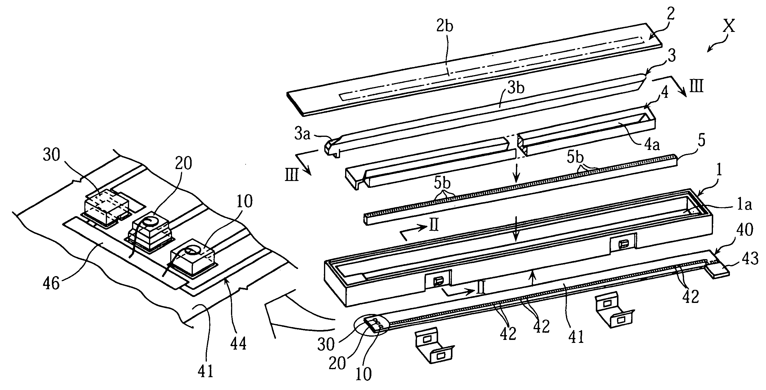
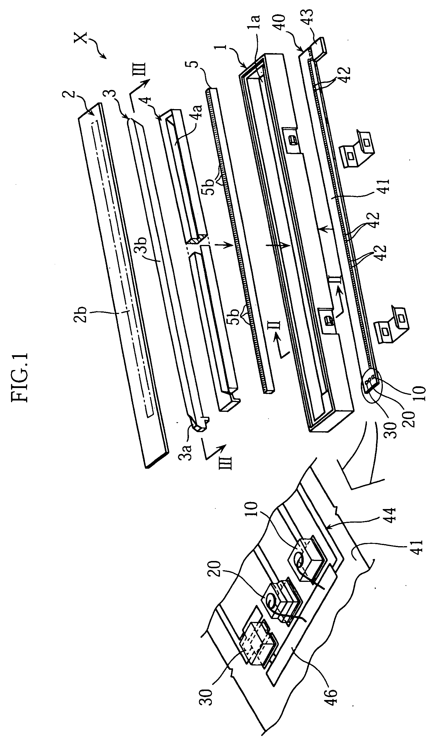
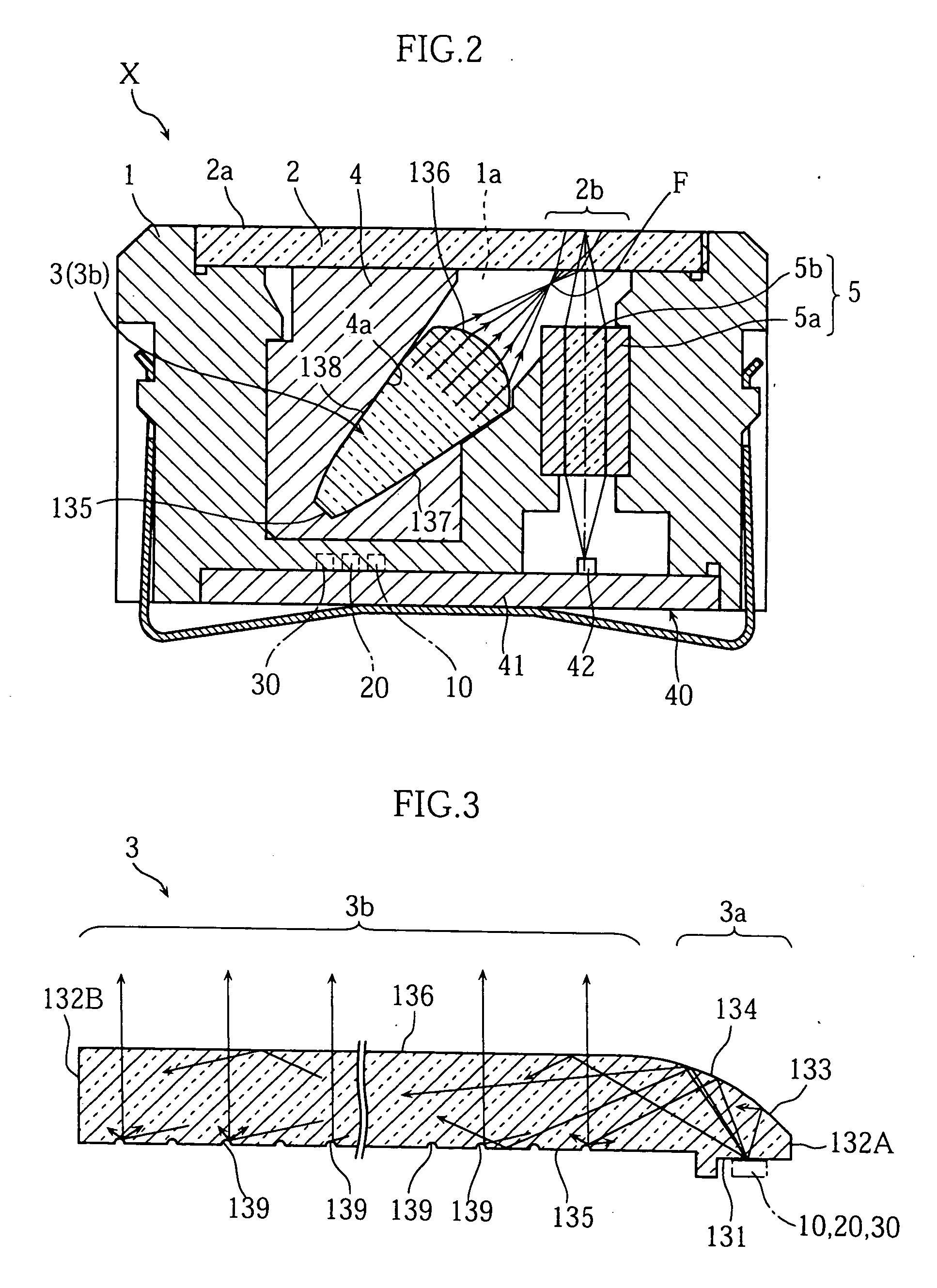
[0046]FIG. 1 is an exploded perspective view of an image reading device X according to the present invention. FIG. 2 is an enlarged cross-sectional view taken along the line II-II shown in the image reading device X of FIG. 1 in an assembled state. The image reading device X comprises a case 1, a circuit board 40, a transparent plate 2, a light guide 3, a reflector 4, and a lens array 5.

[0047] The case 1 is formed into an elongated shape by a synthetic resin or the like to have a predetermined receiving space la. The above-mentioned components constituting the image reading device X are set in the case 1.

[0048] The circuit board 40 comprises a wiring board 41, three LED chips 10, 20 and 30, and a plurality of photoelectric converters 42 that are arranged in a line, where an LED chip mounting structure, as will be described hereinafter, is applied for mounting the LED chips 10, 20 and 30 onto the wiring board 41.

[0049] The wiring board 41 is installed in a bottom surface portion o...


PUM


Abstract

An LED chip mounting structure provided by the present invention includes a wiring board with a mounting pad (45R), an LED chip (10) with an electrode (12) facing the mounting pad (45R), a bump (47) disposed between the mounting pad (45R) and the electrode (10) to electrically connect the mounting pad (45R) to the electrode (10), and an adhesive member (7) for fixing the LED chip (10) to the wiring board (41).

Description

TECHNICAL FIELD [0001] The present invention relates to an LED chip mounting structure constituted by having an LED chip mounted on the wiring board, and an image reading device employing the same. BACKGROUND ART [0002] An image reading device generally comprises a light source and a light receiving portion. The light source emits light to irradiate an image-scanned region, when the reading device is operated. The light emitted from the light source is reflected at the image-scanned region of a document, which is a target of image reading. The light receiving portion receives the reflected light and outputs an image signal in accordance with the amount of light received. In such an image reading device, sometimes three light-emitting diode (LED) chips with different luminescent colors are applied as the light source. In this case, these LED chips are incorporated in the image reading device while being mounted in a predetermined wiring board. [0003]FIG. 10A to FIG. 10C show three LE...

Claims


Application Information

Patent Timeline
IPC IPC(8): G03B27/54H01L21/52H01L33/32H01L33/60H01L33/62H04N1/028
CPCH01L24/32H01L2924/07802H01L2224/48091H01L2224/48227H01L2224/48465H01L2224/73265H01L2924/01029H01L2924/01033H01L2924/01057H01L2924/01078H01L2924/01079H01L2924/01082H01L33/62H01L2224/83851H01L2224/293H01L2224/2929H01L2924/12041H01L2924/0132H01L24/83H01L2224/45144H01L2224/73204H01L2224/32225H01L2224/32145H01L2224/16225H01L2924/01074H01L2924/01006H01L2924/01005H01L2224/92247H01L2224/83192H01L2924/00014H01L2924/00H01L2924/01014H01L2924/3512H01L2224/05573H01L2224/05568H01L24/16H01L2224/06102H01L2224/1703H01L2224/05599
Inventor YOSHIKAWA, YASUHIRO
Owner ROHM CO LTD
Why Eureka
Try Eureka