Aging circuit for organic electro luminescence device and driving method thereof

a luminescence device and organic technology, applied in the direction of static indicating devices, instruments, etc., can solve the problems of low light emission efficiency and brightness of a pdp, high power consumption, and difficult lcd, and achieve the effect of preventing the deterioration of the organic electro luminescence devi

Inactive Publication Date: 2006-12-12
LG DISPLAY CO LTD
View PDF13 Cites 10 Cited by
  • Summary
  • Abstract
  • Description
  • Claims
  • Application Information

AI Technical Summary

Benefits of technology

[0020]Accordingly, it is an object of the present invention to provide an aging circuit for an organic electro luminescence device that is adaptive for preventing the organic electro luminescence device from being deteriorated.

Problems solved by technology

However, the light emission efficiency and brightness of a PDP is low while its power consumption is high.
Compared to a PDP, an LCD is difficult to make because of the semiconductor process for making the Thin Film Transistor (TFT), which is used as a switching device in each of the pixels in the LCD.
However, the LCD has a disadvantage in that power consumption is high because the LCD uses a backlight unit.
Further, the LCD also has the disadvantage of high light loss caused by the use of optical devices, such as a polarizing filter, a prism sheet, a diffusion panel.
Another disadvantage of the LCD is a narrow viewing angle.
In the organic electro luminescence device as discussed the above, there is a disadvantage in that the switching performance of the switching transistors TFT T1 and TFT T2 deteriorates over time.

Method used


Image

  • Aging circuit for organic electro luminescence device and driving method thereof
  • Aging circuit for organic electro luminescence device and driving method thereof
  • Aging circuit for organic electro luminescence device and driving method thereof

Examples


first embodiment

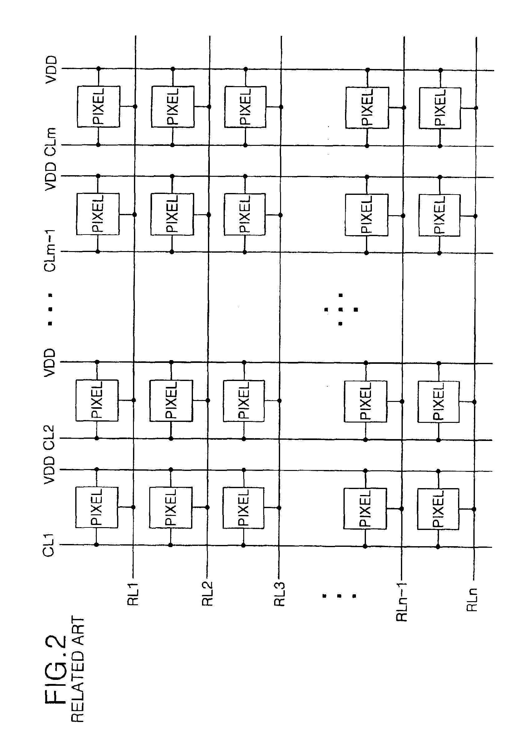
[0036]FIG. 6 is a diagram representing an aging circuit for an organic electro luminescence device according to the present invention. As shown in FIG. 6, the organic electro luminescence device according to the present embodiment includes a number m of column lines CL1 to CLm, a number n of row lines RL1 to RLn to cross the column lines CL1 to CLm, a number m×n of pixels 42 arranged in a matrix at intersection parts, and an aging circuit 44 enabling the size of the aging voltages and an aging voltage application time to vary, so that aging can be implemented correctly and effectively to improve all characteristics of the organic electro luminescence device, such as the brightness and the deterioration prevention of switch devices.

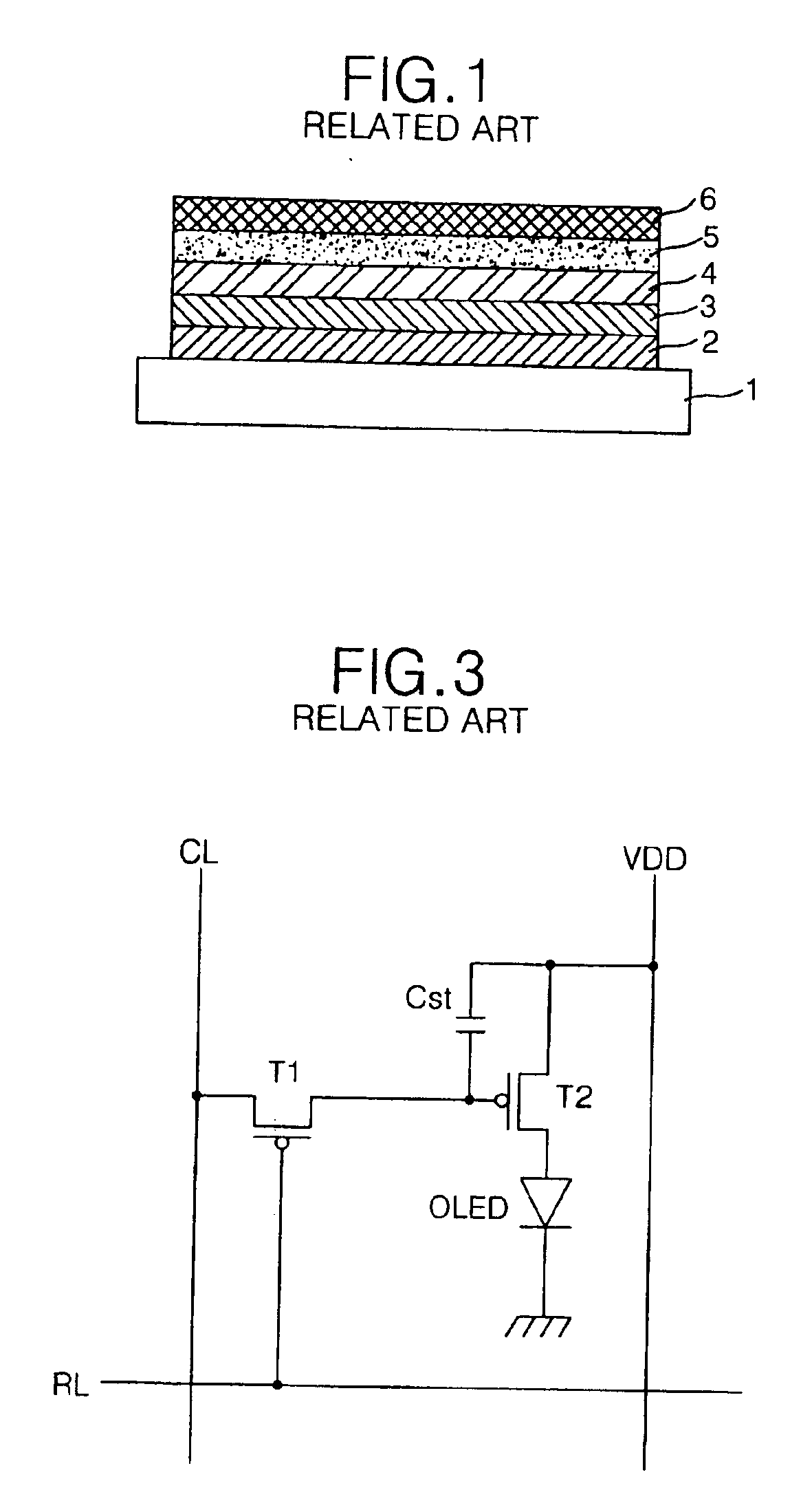
[0037]Each pixel 42 includes a first TFT T1 acting as a switching device formed at each intersection part of the column lines CL1 to CLm and the row lines RL1 to RLn, a second TFT T2 formed between a cell drive voltage source VDD and an electro luminescenc...

second embodiment

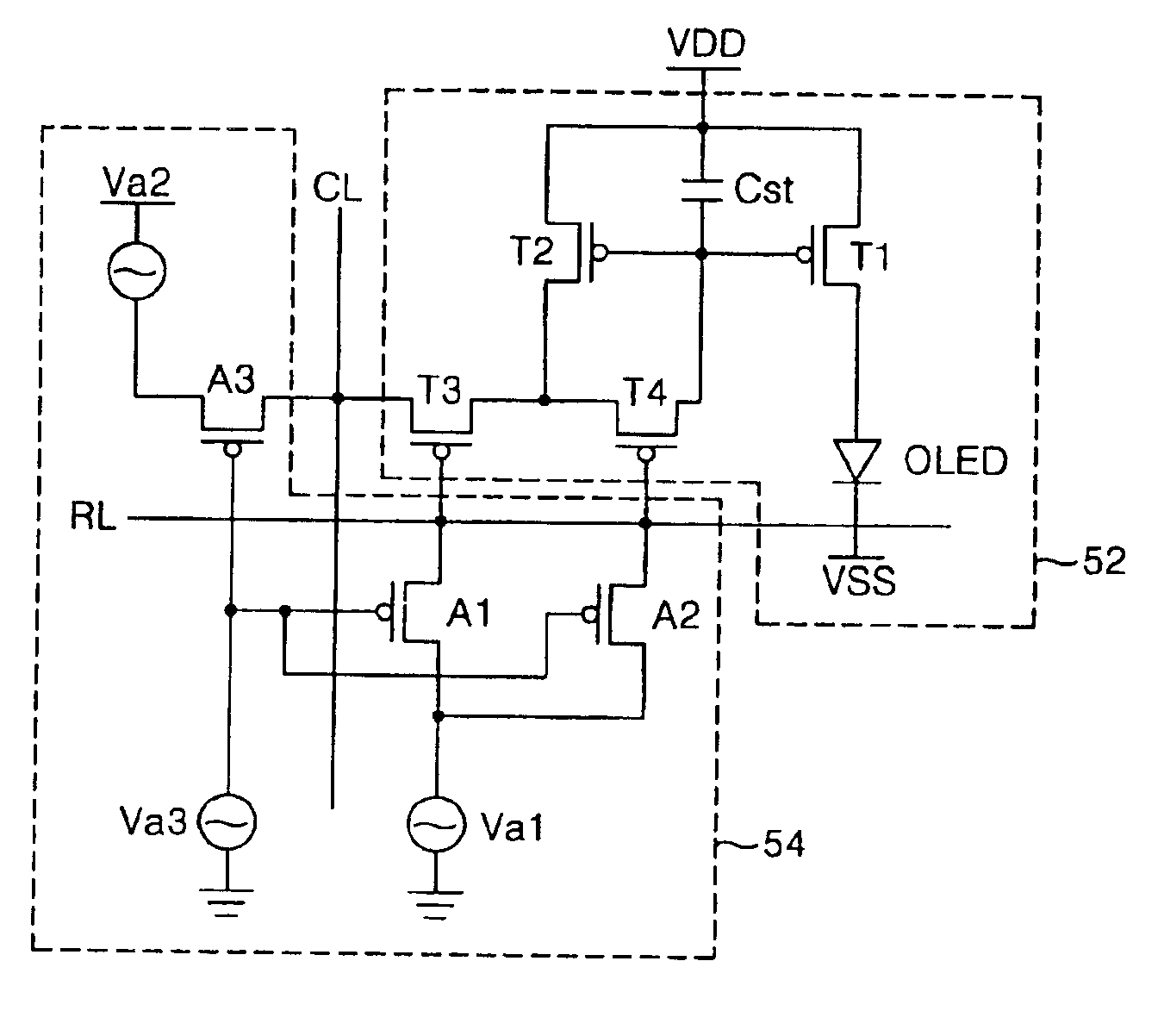
[0045]FIG. 8 is a diagram representing an aging circuit for an organic electro luminescence device according to the present invention. As shown in FIG. 8, the organic electro luminescence device includes a number m of column lines CL1 to CLm, a number n of row lines RL1 to RLn to cross the column lines CL1 to CLm, a number m×n of pixels 52 arranged in a matrix at intersection parts, and an aging circuit 54 enabling the size of voltage and a voltage application time to vary, so that aging can be implemented correctly and effectively for improving all characteristics of the organic electro luminescence device, such as the brightness of organic electro luminescence cell OLED and to prevent deterioration of switching devices.

[0046]Each pixel 52 includes a first TFT T1 formed between a cell drive voltage source VDD and an electro luminescence cell OLED for driving the electro luminescence cell OLED; a second TFT T2 connected to the cell drive voltage source VDD to form a current mirror w...


PUM


Abstract

An aging circuit for an organic electro luminescence device includes a plurality of pixels arranged in a matrix at intersection areas of row lines and column lines and an aging circuit having at least one aging AC voltage source to apply a specific aging AC voltage pulse to the pixels.

Description

[0001]This application claims the benefit of the Korean Patent Application No. P02-050880 filed on Aug. 27, 2002, which is hereby incorporated by reference.BACKGROUND OF THE INVENTION[0002]1. Field of the Invention[0003]The present invention relates to an electro luminescence device, and more particularly to an aging circuit for an organic electro luminescence device to prevent the deterioration of the electro luminescence device, and a driving method thereof.[0004]2. Description of the Related Art[0005]Recently, there has been developed various flat panel displays, which have the advantages of reduced weight and reduced bulk over a Cathode Ray Tube (CRT). Such flat panel displays include a Liquid Crystal Display (LCD), a Field Emission Display (FED), a Plasma Display Panel (PDP), and Electro Luminescence (hereinafter, EL) display device.[0006]The structure and fabricating process of the PDP are relatively simple compared to the LCD, FED and EL devices. Another advantage of the PDP ...

Claims


Application Information

Patent Timeline
Patent Type & Authority Patents(United States)
IPC IPC(8): G09G3/10G09G3/30G09G3/00G09G3/32
CPCG09G3/006G09G3/3233G09G3/3241G09G3/3283G09G3/3291G09G2300/0814G09G2300/0842G09G2310/0254G09G2310/0256G09G2310/0297G09G2320/02G09G2320/043G09G3/30
Inventor HA, YONG MINKIM, CHANG YEONHAN, SANG SOO
Owner LG DISPLAY CO LTD
Why Eureka
Try Eureka