

Plasma display and method of producing phosphor used therein
a technology of phosphor and display device, which is applied in the manufacture of electric discharge tubes/lamps, discharge tubes luminescnet screens, lighting and heating apparatus, etc., can solve the problems of uneven coating, clogging of nozzles, uneven coating, etc., to prevent the degradation of luminance of phosphor, improve the life and reliability of pdp, and improve the luminance. the effect of phosphor degradation
Inactive Publication Date: 2008-09-09
PANASONIC CORP
View PDF9 Cites 8 Cited by
- Summary
- Abstract
- Description
- Claims
- Application Information
AI Technical Summary
Benefits of technology
This approach improves the luminance, life, and reliability of plasma display devices by preventing luminance degradation and clogging, ensuring even coating and enhanced discharge characteristics.
Problems solved by technology
Large agglomerates are included in a phosphor unless the phosphor particles are classified after being lightly crushed, and thus unevenness in coating and clogging in the nozzle may occur when coating with the pasted phosphors.
Further, it is known that ink-jet coating, in which coating is made continuously using negatively charged ink for a green phosphor through a fine-bore nozzle, causes clogging in the nozzle and unevenness in coating.
Further, there is a problem in which a negatively charged phosphor causes ion collision of positive ions of Ne, CH-base, or H occurring while discharging with a negatively charged green phosphor, thus deteriorating the luminance of the phosphor.
However, it is problematic that laminate-coating oxide causes a low luminance, and applying two different kinds of phosphor with a charge state different from each other tends to generate clogging and unevenness in coating.
Method used
View moreImage
Smart ImageViewing Examples

Examples
experiment 1
[0082]A measurement is made of the charging tendency for the green phosphors in samples 1 through 9 and comparative sample 10. Here, the measurement adopts blow-off method, which measures the amount of charge for reduced iron powder.
experiment 2
[0083]A measurement is made of the element ratio of Zn to Si at the proximity (approximately 10 nm in depth) of the surface with X-Ray photoelectron spectroscopy (XPS) for samples 1 through 9 and comparative sample 10 produced.
experiment 3
[0084]A measurement is made of the luminance of a PDP when displaying full white after the PDP producing process, and the luminance of green and blue phosphor layers, with a luminance meter.
Login to View More PUM
| Property | Measurement | Unit |
|---|---|---|
| temperature | aaaaa | aaaaa |
| particle diameter | aaaaa | aaaaa |
| particle diameter | aaaaa | aaaaa |
Abstract
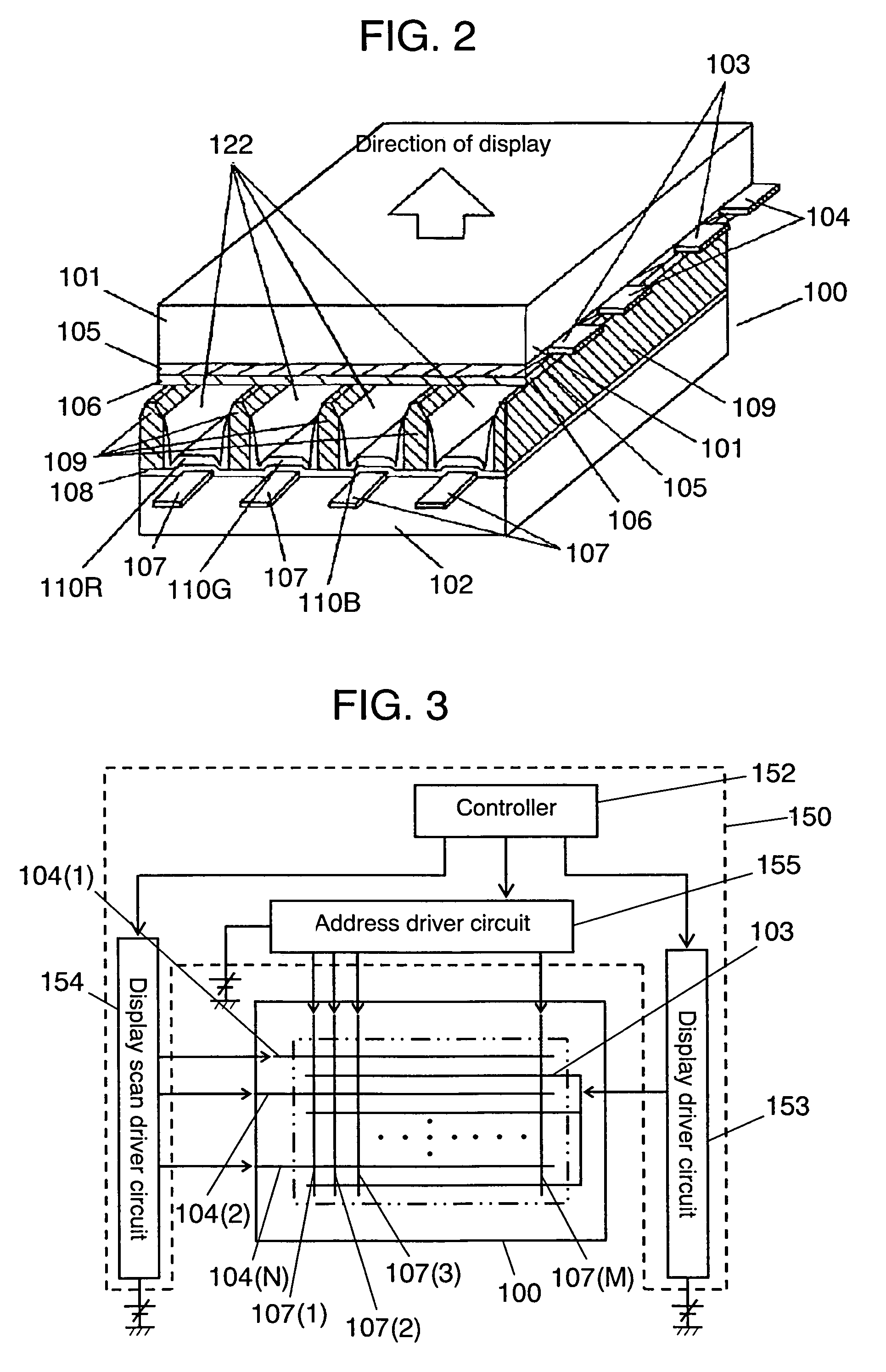
The present invention relates to a plasma display device and to a method of producing a phosphor to be used for the device, that prevents the phosphor layer from deteriorating, and improves the luminance, life, and reliability, of a plasma display panel (PDP). The plasma display device is equipped with a plasma display panel in which a plurality of discharge cells are arranged, phosphor layers (110R, 110G, 110B) in color corresponding to each discharge cell are disposed, and phosphor layers (110R, 110G, 110B) are excited by ultraviolet light to emit light. Green phosphor layer (110G) has a green phosphor including Zn2SiO4:Mn, the element ratio of zinc (Zn) to silicon (Si) at the proximity of its surface is 2 / 1, which is the stoichiometric ratio, and the layer is positively charged or zero-charged.
Description
[0001]This application is a U.S. National Phase Application of PCT International Application PCT / JP2004 / 014415.TECHNICAL FIELD[0002]The present invention relates to a plasma display device having phosphor layers that are excited by ultraviolet light to emit light, and to a method of producing a phosphor used for the device.BACKGROUND ART[0003]In recent years, plasma display devices using plasma display panels (hereinafter, referred to as “PDP” or “panel”) receive attention as color display devices that implement a large screen size, a thin body, and a light weight in displaying color images for computers, television sets, and the like.[0004]A plasma display device displays full color by means of additive color mixing of so-called three primary colors (red, green, and blue). For displaying full color, a plasma display device is provided with phosphor layers that emit light in the three primary colors: red (R), green (G), and blue (B). Phosphor particles composing the phosphor layers ...
Claims
Login to View More Application Information
Patent Timeline
 Patent Type & AuthorityPatents(United States)
IPC IPC(8): C09K11/59H01J17/49C09K11/08C09K11/54C09K11/77C09K11/78C09K11/79H01J9/227H01J11/12H01J11/22H01J11/24H01J11/26H01J11/34H01J11/42
CPCC09K11/592C09K11/7797C09K11/7734H01J2211/42C09K11/54C09K11/77H01J11/42
InventorMIYAMAE, YUICHIROAOKI, MASAKISUGIMOTO, KAZUHIKOHORIKAWA, KEIJIHIBINO, JUNICHIYOSHINORI, TANAKAHIROSHI, SETOGUCHI
OwnerPANASONIC CORP