Semiconductor light emitting device and fabrication method thereof

a technology of light emitting device and semiconductor, which is applied in the direction of semiconductor device, basic electric element, electrical apparatus, etc., can solve the problems of reducing the size of light emitting element, and partially degrading the directivity, so as to reduce the size of the light emitting element

Active Publication Date: 2005-10-27
LEDCOMM LLC
View PDF6 Cites 45 Cited by
  • Summary
  • Abstract
  • Description
  • Claims
  • Application Information

AI Technical Summary

Benefits of technology

[0014] An object of the present invention is to provide a semiconductor light emitting device having a light emitting element mounted on a lead frame, directed to reducing the size thereof while allowing adjustment of the directivity of output light, or ensuring the strength of the lead frame, and a fabrication method of such a semiconductor light emitting device.

Problems solved by technology

There is a possibility of the adjustment of the directivity being partially degraded when the light emitting element is reduced in size.
As a result, there are cases where reduction in the size of the light emitting element is restricted.
As a result, there are cases where reduction in size of the light emitting element is restricted.

Method used


Image

  • Semiconductor light emitting device and fabrication method thereof
  • Semiconductor light emitting device and fabrication method thereof
  • Semiconductor light emitting device and fabrication method thereof

Examples


Embodiment Construction

[0039] Embodiments of a semiconductor light emitting device and a fabrication method thereof according to the present invention will be described hereinafter with reference to FIGS. 1-6.

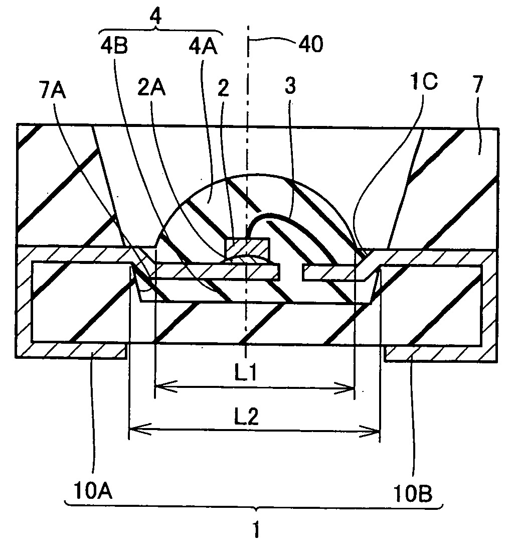
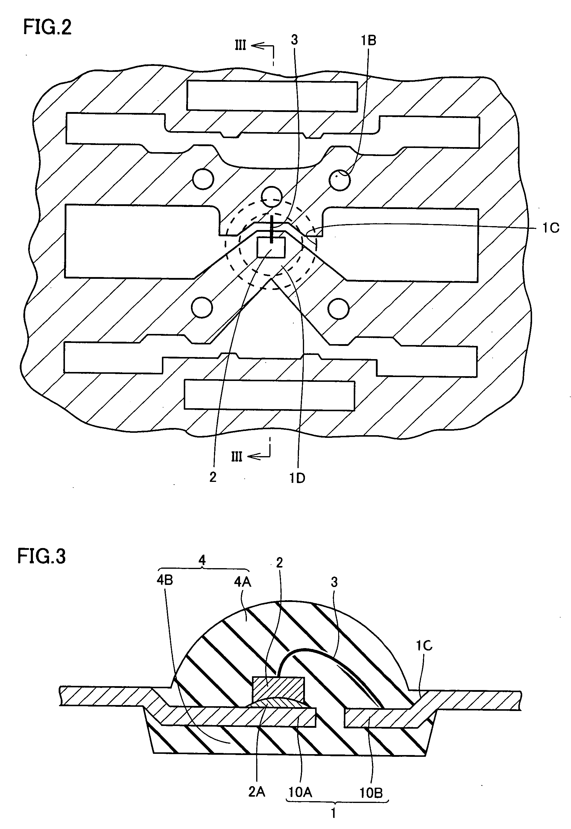
[0040] Referring to FIG. 5, a semiconductor light emitting device according to an embodiment of the present invention includes an LED element 2 (semiconductor light emitting element), a lead frame 10A (first lead frame) on which LED element 2 is mounted, a lead frame 10B (second lead frame) electrically connected to LED element 2 via a wire 3, transparent resin 4 (light transmitting resin) formed on LED element 2 and lead frame 1 (10A, 10B), and light shielding resin 7 (resin that blocks light) having a reflectance higher than that of transparent resin 4, and surrounding the perimeter of LED element 2. Transparent resin 4 includes a lens portion 4A constituting a lens on LED element 2, and a holding portion 4B holding lead frame 1.

[0041] The leading end of lead frame 1 is inserted into transparent ...


PUM


Abstract

A semiconductor light emitting device includes an LED element, a lead frame on which the LED is mounted, a lead frame electrically connected to the LED element via a wire, transparent resin formed on the LED element and on the lead frames, and light shielding resin having a reflectance higher than the reflectance of the transparent resin, surrounding the perimeter of the LED. The transparent resin includes a lens portion constituting a lens on the LED, and a holding portion holding the lead frame.

Description

[0001] This nonprovisional application is based on Japanese Patent Application No. 2004-131774 filed with the Japan Patent Office on Apr. 27, 2004, the entire contents of which are hereby incorporated by reference. BACKGROUND OF THE INVENTION [0002] 1. Field of the Invention [0003] The present invention relates to a semiconductor light emitting device, and a method of fabricating such a semiconductor light emitting device. Particularly, the present invention relates to a semiconductor light emitting device employing a light emitting element such as an LED (Light Emitting Diode), and a method of fabricating such a semiconductor light emitting device. [0004] 2. Description of the Background Art [0005] Semiconductor light emitting devices employing a light emitting element such as an LED are conventionally known. [0006] For example, Japanese Patent Laying-Open No. 11-087780 (first conventional example) discloses a light emitting device including a light emitting element, a lead frame o...

Claims


Application Information

Patent Timeline
Patent Type & Authority Applications(United States)
IPC IPC(8): H01L29/22H01L33/54H01L33/56H01L33/62
CPCH01L33/486H01L2924/12041H01L33/62H01L33/647H01L2224/48091H01L2224/48247H01L2224/73265H01L2924/01004H01L2924/3025H01L33/54H01L24/97H01L2224/32245H01L2224/97H01L2924/00014H01L2924/00H01L2924/181H01L2924/00012
Inventor ABE, MUNEZOYOSHIDA, TOSHIHIKO
Owner LEDCOMM LLC
Why Eureka
Try Eureka