Four phase charge pump operable without phase overlap with improved efficiency
- Summary
- Abstract
- Description
- Claims
- Application Information
AI Technical Summary
Benefits of technology
Problems solved by technology
Method used
Image
Examples
Embodiment Construction
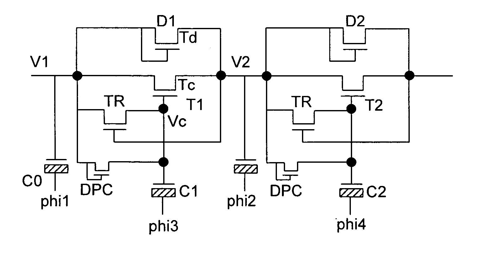
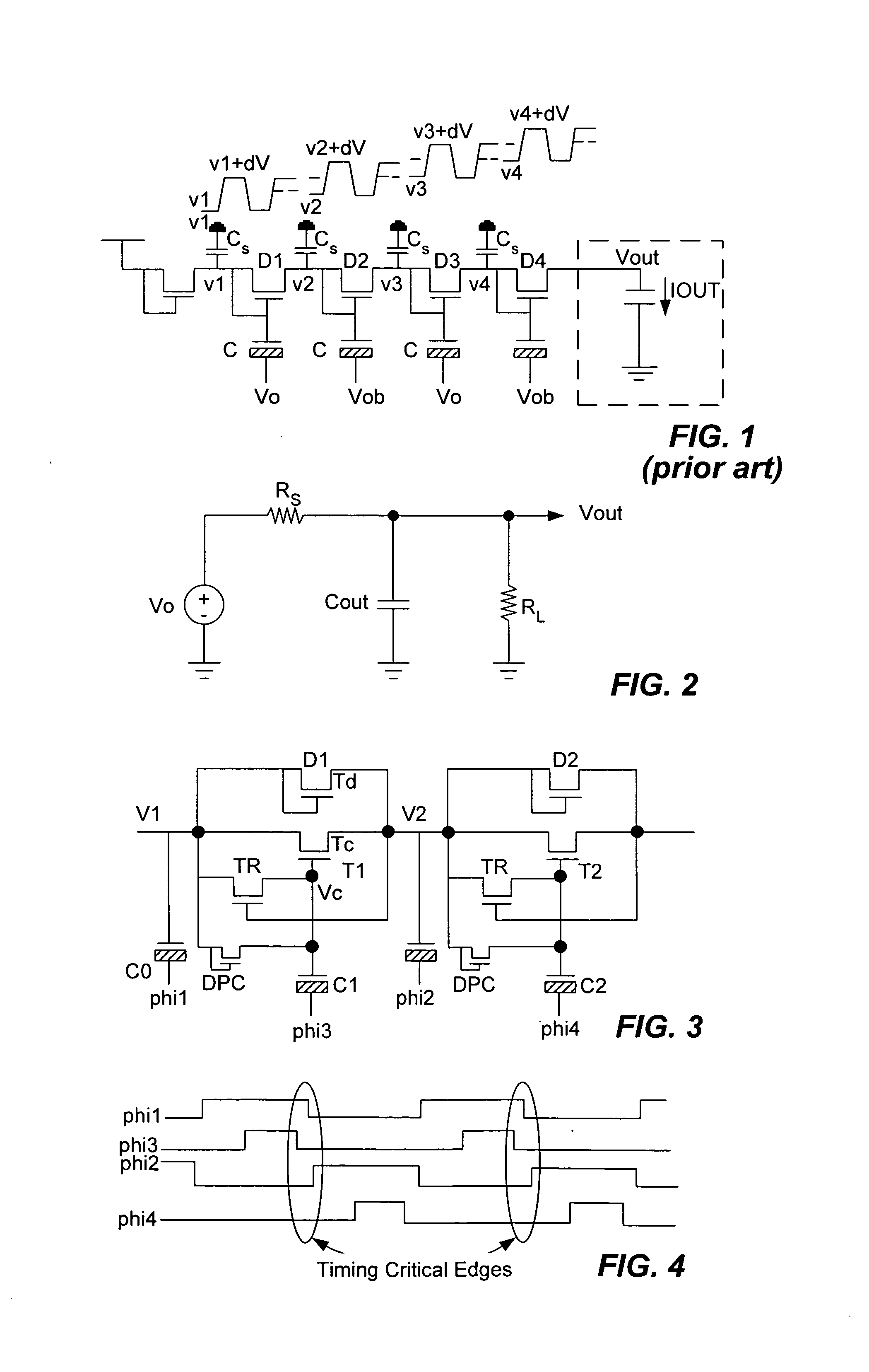
[0014]FIG. 3 is a schematic of a charge pump in accordance with one embodiment of the invention in which the cells of the conventional Dickson charge pump are modified to facilitate charge transfer and to accommodate a higher clock frequency or fosc. FIG. 3 shows two adjacent cells, such as diodes D1 and D2 of the Dickson charge pump of FIG. 1, for transferring charge from node V1 to node V2. Each cell is modified by providing a MOS transistor T1 or T2 in parallel with diode D1 or diode D2 which facilitate the transfer of residual trapped charge at each node. A recovery transistor TR is connected between the gate of transistor T1 and node V1 with the gate of transistor TR controlled by the voltage on node V2. When charge is transferred from node V1 to node V2, the increased voltage at node V2 causes transistor TR to conduct and bring the voltage on the gate of transistor T1 to the voltage level of node V1. After clock φ3 is removed, the conductance of transistor T1 is terminated.
[0...
PUM
 Abstract
Description
Claims
Application Information


