Supercharge Your Innovation With Domain-Expert AI Agents!

Integrated optics and electronics

a technology of optics and electronics, applied in multiplex communication, semiconductor lasers, instruments, etc., can solve the problem of higher product cos

Inactive Publication Date: 2005-12-01
AVAGO TECH INT SALES PTE LTD
View PDF63 Cites 15 Cited by
  • Summary
  • Abstract
  • Description
  • Claims
  • Application Information

AI Technical Summary

Benefits of technology

The invention is an optoelectronic device that includes a submount and a lid. The submount has a lens and a laser, while the lid has a cavity with a surface coated with a reflective material to form a 45 degree mirror. The mirror reflects light from the laser to the lens, which then exits the device through the submount. The technical effect of this invention is that it allows for more efficient and precise light manipulation in the optoelectronic device.

Problems solved by technology

This means of assembly is often slow and labor intensive, resulting in higher product cost.

Method used


Image

  • Integrated optics and electronics
  • Integrated optics and electronics
  • Integrated optics and electronics

Examples


Embodiment Construction

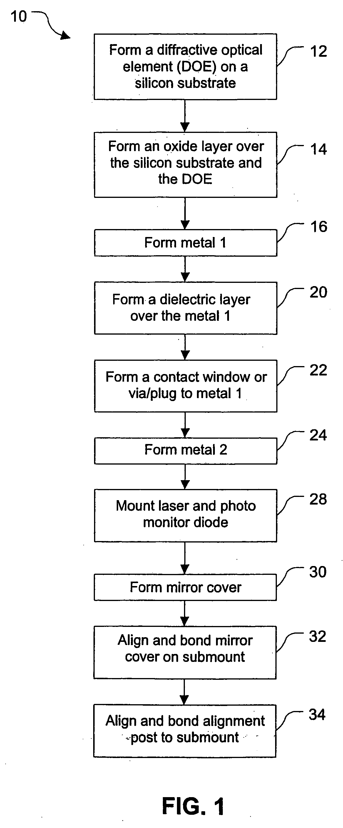
[0018] An optoelectronic package may include a submount wafer, a ring wafer bonded to the submount wafer, and a lid wafer bonded to the ring wafer. The lid wafer typically includes an integrated lens. The submount wafer typically includes an edge-emitting laser and interconnects for powering the laser. The ring wafer is typically processed using RIE etching to form straight walls. An additional component that has a 45 degree surface is placed next to the laser inside the ring. This component acts as a mirror to reflect the light from the laser up through the lens in the lid. Alternatively, the ring wafer is processed to form an integrated 45 degree mirror that reflects the light from the laser up through the lens in the lid wafer.

[0019] The optoelectronic package requires two hermetic seals: one between the ring wafer and the lid wafer, and another between the ring wafer and the submount wafer. In the case where there is an additional mirror component, that too has to be aligned an...


PUM


Abstract

An optoelectronic device includes a submount and a lid. The submount includes a substrate and a lens and a laser above the substrate. The lid defines a cavity having a surface coated with a reflective material to form a 45 degree mirror. The mirror reflects a light from the laser to the lens and the light exits the optoelectronic device through the submount.

Description

FIELD OF INVENTION [0001] This invention relates to a wafer-scale package for an optoelectronic device, and more specifically to a wafer-scale submount for an optoelectronic device. DESCRIPTION OF RELATED ART [0002] Optoelectronic (OE) devices are generally packaged as individual die. This means of assembly is often slow and labor intensive, resulting in higher product cost. Thus, what is needed is a method to improve the packaging of OE devices. SUMMARY [0003] In one embodiment of the invention, an optoelectronic device includes a submount and a lid. The submount includes a lens and a laser above a substrate. The lid defines a cavity having a surface coated with a reflective material to form a 45 degree mirror. The mirror reflects a light from the laser to the lens and the light exits the optoelectronic device through the submount.BRIEF DESCRIPTION OF THE DRAWINGS [0004]FIG. 1 is a flowchart of a method 10 for making an optoelectronic device including a submount, a lid, and an alig...

Claims


Application Information

Patent Timeline
Patent Type & Authority Applications(United States)
IPC IPC(8): H01S5/022G02B6/12G02B6/42H01L33/00H01S3/04H01S5/00H01S5/02H01S5/026H04J14/08
CPCG02B6/4214G02B6/4292H01S5/02252H01S5/4025H01S5/02292H01S5/0683H01S5/02284H01S5/02251H01S5/02255H01S5/02326
Inventor GALLUP, KENDRA J.MATTHEWS, JAMES ALBERT
Owner AVAGO TECH INT SALES PTE LTD
Features
  • R&D
  • Intellectual Property
  • Life Sciences
  • Materials
  • Tech Scout
  • Unparalleled Data Quality
  • Higher Quality Content
  • 60% Fewer Hallucinations
Learn More