

Ribbon bonding in an electronic package
a technology of electronic packaging and bonding, which is applied in the direction of manufacturing tools, non-electric welding apparatus, and capacitors, etc., can solve the problems of increasing the thickness of metalized parts, increasing the cost by decreasing the throughput of wafer/die manufacturing process, and limited wires, so as to reduce processing steps and time to produce the connection, reduce the overall volume of the connection, and increase the cross section and contact area
- Summary
- Abstract
- Description
- Claims
- Application Information
AI Technical Summary
Benefits of technology
Problems solved by technology
Method used
Image

Examples
Embodiment Construction
[0034] According to one aspect of the present invention, one or more conductive flexible ribbons are used to electrically connect a semiconductor die to a lead frame.
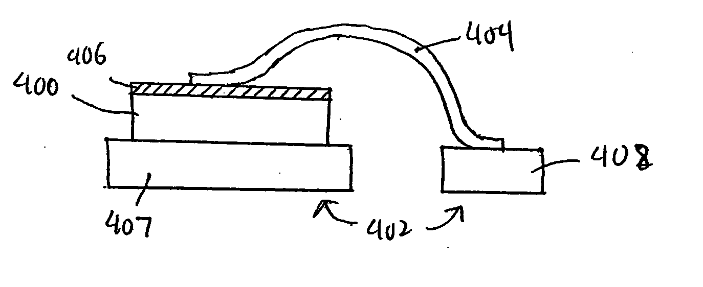
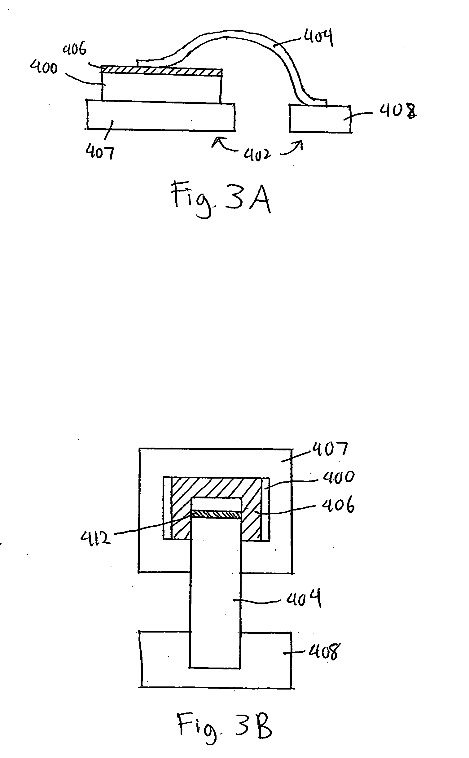
[0035]FIGS. 3A and 3B show a side view and top view of a semiconductor die 400 coupled to a lead frame 402 by a conductive flexible ribbon 404, according to one embodiment of the invention. Die 400 includes a metalized portion 406, such as aluminum, that provides connection to underlying elements of die 400. Die 400, in one embodiment, is part of a power semiconductor device, such as a power MOSFET. Lead frame 402 includes a support portion 407 to which die 400 is secured, e.g., by solder or epoxy, and terminals 408 that allow electrical connection to external devices. An enclosure, covering, or package protects the die from external elements. In some embodiments, the semiconductor package is a TO-220 or an SO-8 package.
[0036] Ribbon 404, which may have a rectangular cross section, is aluminum, although other conducti...
PUM
| Property | Measurement | Unit |
|---|---|---|
| thickness | aaaaa | aaaaa |
| diameter | aaaaa | aaaaa |
| width | aaaaa | aaaaa |
Abstract
Description
Claims
Application Information