Package for semiconductor light emitting element and semiconductor light emitting device

a technology of light emitting elements and semiconductors, applied in semiconductor devices, semiconductor/solid-state device details, electrical devices, etc., can solve the problems of difficult connection of electrodes when provided on the top surface, large heat generation of leds, and insufficient heat generation of semiconductor light emitting devices alon

Inactive Publication Date: 2005-12-22
KK TOSHIBA
View PDF4 Cites 33 Cited by
  • Summary
  • Abstract
  • Description
  • Claims
  • Application Information

AI Technical Summary

Benefits of technology

[0011] Aspects of the present invention address one or more issues described above, thereby providing an improved LED.

Problems solved by technology

The LEDs generate large amounts of heat because they are driven by large currents.
Semiconductor light emitting devices alone do not radiate heat well.
In the case a plurality of light emitting devices is arrayed and connected each other, it is hard to connect their electrodes when provided on the top surface.

Method used


Image

  • Package for semiconductor light emitting element and semiconductor light emitting device
  • Package for semiconductor light emitting element and semiconductor light emitting device
  • Package for semiconductor light emitting element and semiconductor light emitting device

Examples


first embodiment

The First Embodiment

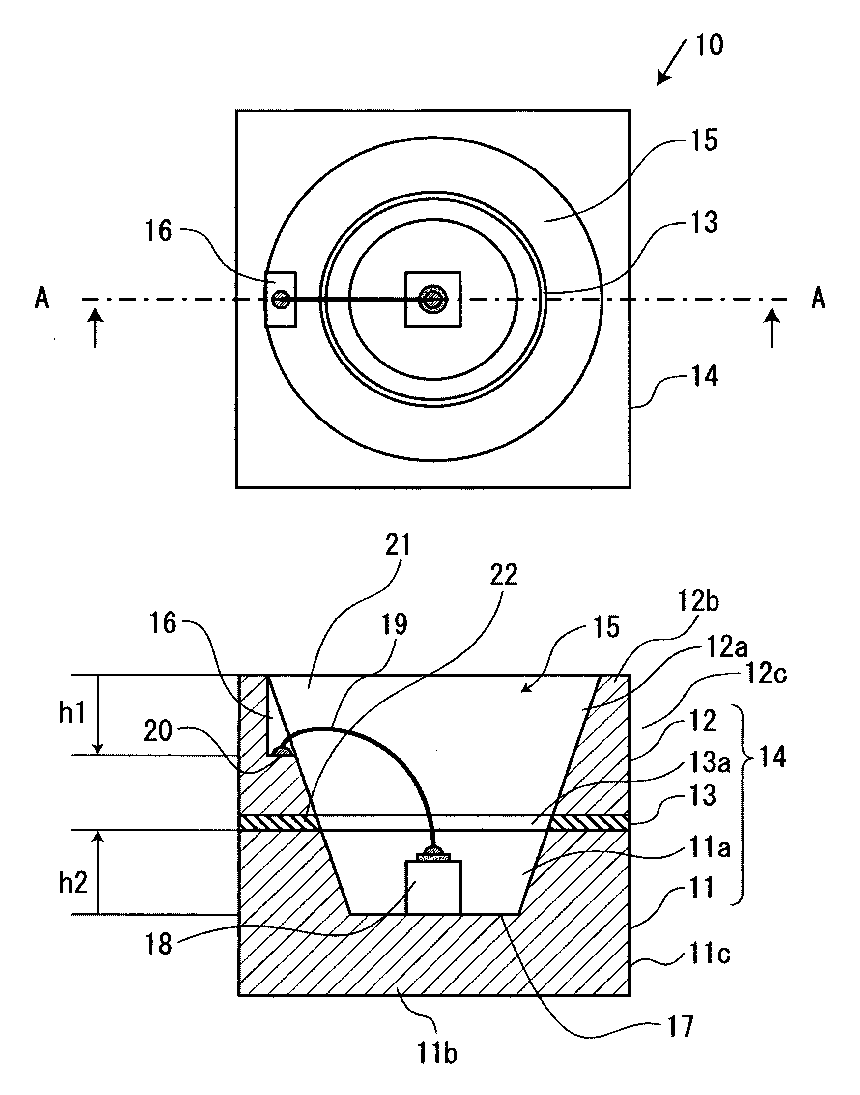
[0025] A first embodiment of the present invention will be explained with reference to FIG. 1A to FIG. 5. FIG. 1A is a plane view of a package for semiconductor light emitting element according to a first embodiment of the present invention. FIG. 1B is a cross sectional view taken along A-A line and seen to the arrow in FIG. 1A of a package for semiconductor light emitting element according to a first embodiment of the present invention.

[0026] As shown in FIG. 1A and FIG. 1B, a package for semiconductor light emitting element 10 according to this embodiment has a substrate 14, cup shaped portion 15, which is formed in substrate 14, and a cavity 20, which is formed in an inner surface 22 of substrate 14.

[0027] Cup shaped portion 15, which has a larger opening than bottom area. Inner surface 22 is slanted.

[0028] Substrate 14 is formed by stacking a first metal substrate 11, an insulating member 13 and a second metal substrate 12 in this order. First metal substr...

second embodiment

The Second Embodiment

[0068] A second embodiment of the present invention will be explained with reference to FIG. 6A to FIG. 7. FIG. 6A is a plane view of a package for semiconductor light emitting device according to a second embodiment of the present invention, and FIG. 6B is a cross sectional view of a package for semiconductor light emitting element according to a second embodiment of the present invention.

[0069] With respect to each portion of this second embodiment, the same portion of the package for semiconductor light emitting device of the first embodiment shown in FIG. 1A to FIG. 5 is designated by the same reference numeral, and its explanation is omitted.

[0070] The structure of this embodiment will be explained with reference to FIG. 6A and FIG. 7 hereinafter. The package for semiconductor light emitting device according to this embodiment has protrusion on the top surface of its substrate.

[0071] As shown in FIG. 6B, package for semiconductor light emitting device 50...


PUM


Abstract

A package for semiconductor light emitting element is described. The package includes a first metal substrate having a cup shaped recess portion, an insulating member having a first cup shaped opening, provided on the first metal substrate, and a second metal substrate having a second cup shaped opening, provided on the insulating member with being electrically insulated from the first metal substrate, having a cavity in the inner surface.

Description

CROSS REFERENCE TO RELATED APPLICATION [0001] This application is based upon and claims the benefit of priority from the prior Japanese Patent Application No. 2004-183156, filed on Jun. 22, 2004; the entire contents of which are incorporated herein by reference.BACKGROUND OF THE INVENTION [0002] A semiconductor light emitting element, especially light emitting diode (LED), is used for various purposes such as full color displays, traffic signals, and lights for vehicles. These applications require high light output. [0003] High luminous flux LEDs, which are driven by large current over several hundred mA, are watched with keen interest. The LEDs generate large amounts of heat because they are driven by large currents. Semiconductor light emitting devices alone do not radiate heat well. [0004] A conventional package for semiconductor light emitting device which has a structure of heat radiation is shown in FIG. 1 and its associated description in the Japanese patent laid open No. 200...

Claims


Application Information

Patent Timeline
Patent Type & Authority Applications(United States)
IPC IPC(8): H01L29/24H01L33/58H01L33/62H01L33/64
CPCH01L33/486H01L33/60H01L33/62H01L2224/48091H01L2924/01322Y10S257/924H01L2924/12041H01L2924/01019H01L2924/01078H01L2924/00014H01L2224/48464
Inventor KONNO, KUNIAKI
Owner KK TOSHIBA
Why Eureka
Try Eureka