Semiconductor device with base support structure

a technology of semiconductor devices and support structures, applied in the direction of semiconductor devices, semiconductor/solid-state device details, radiation control devices, etc., can solve the problems of increasing the cost of equipment and technology required to fabricate such highly integrated chips with each new generation of smaller devices

Inactive Publication Date: 2005-12-22
BESANG
View PDF15 Cites 268 Cited by
  • Summary
  • Abstract
  • Description
  • Claims
  • Application Information

AI Technical Summary

Benefits of technology

[0008] The present invention further provides a semiconductor chip with an acceptor substrate which carries electronic circuitry. An interconnect region is carried by the acceptor substrate. A base support structure is carried by the interconnect region. One or more device structure(s) are carried by the base support structure. A first conductive region is coupled between the base support structure and the electronic circuitry. A second conductive region is coupled between a corresponding device structure and the electronic circuitry.

Problems solved by technology

These laterally oriented devices consume significant amounts of chip area.
However, the equipment and technologies required to fabricate such highly integrated chips becomes increasingly expensive with each new generation of smaller devices.

Method used


Image

  • Semiconductor device with base support structure
  • Semiconductor device with base support structure
  • Semiconductor device with base support structure

Examples


Embodiment Construction

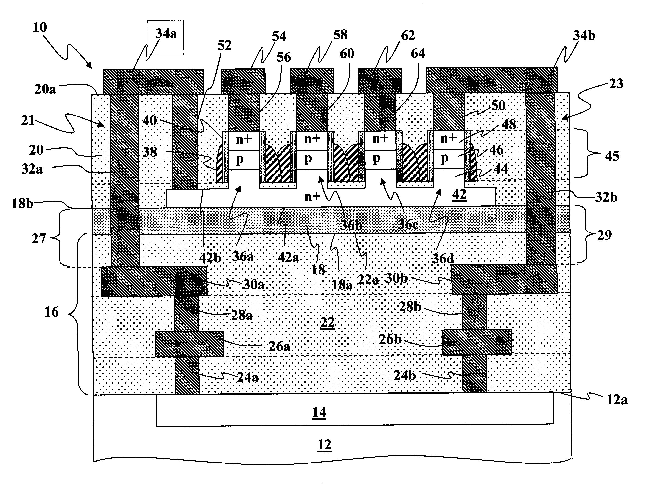
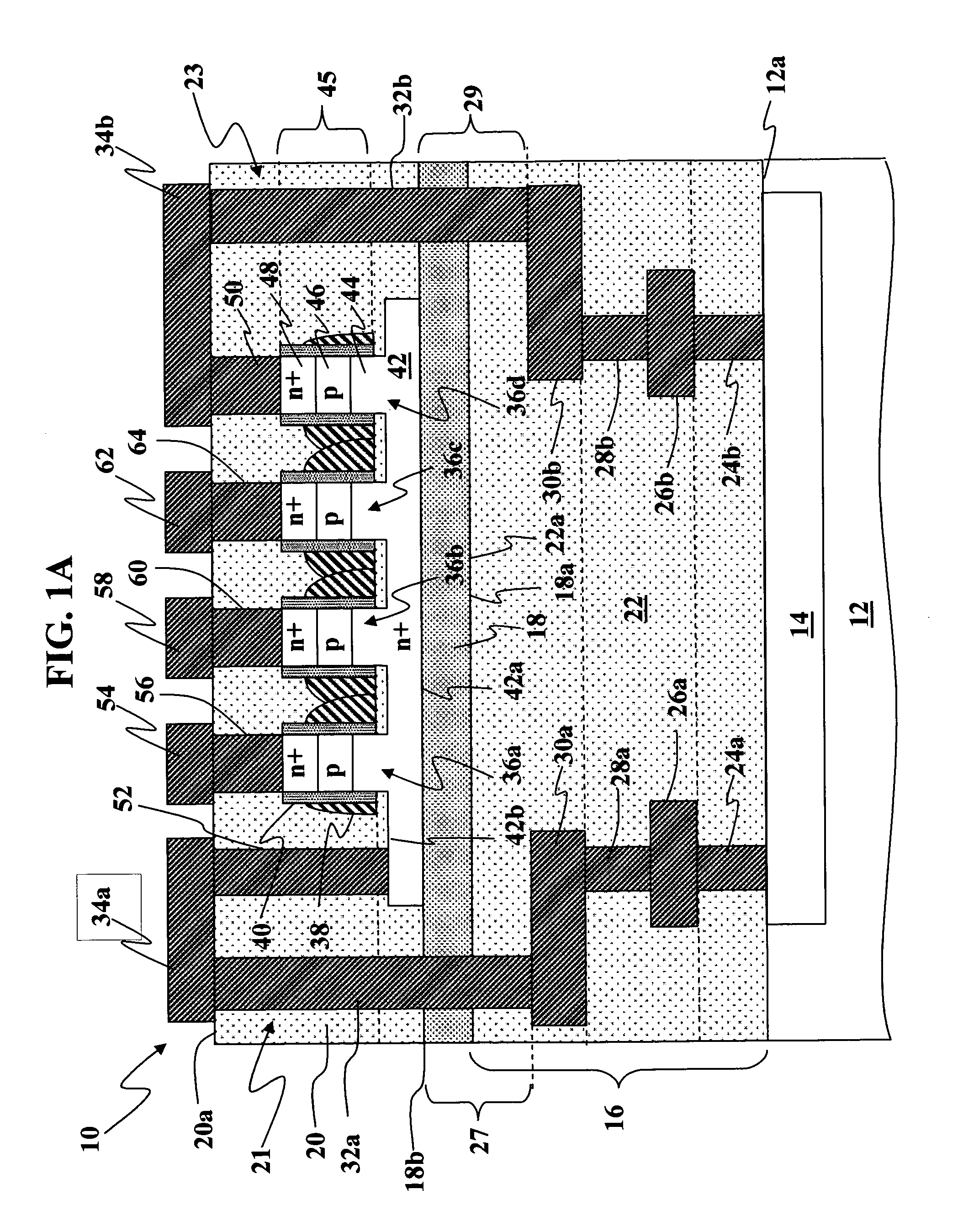
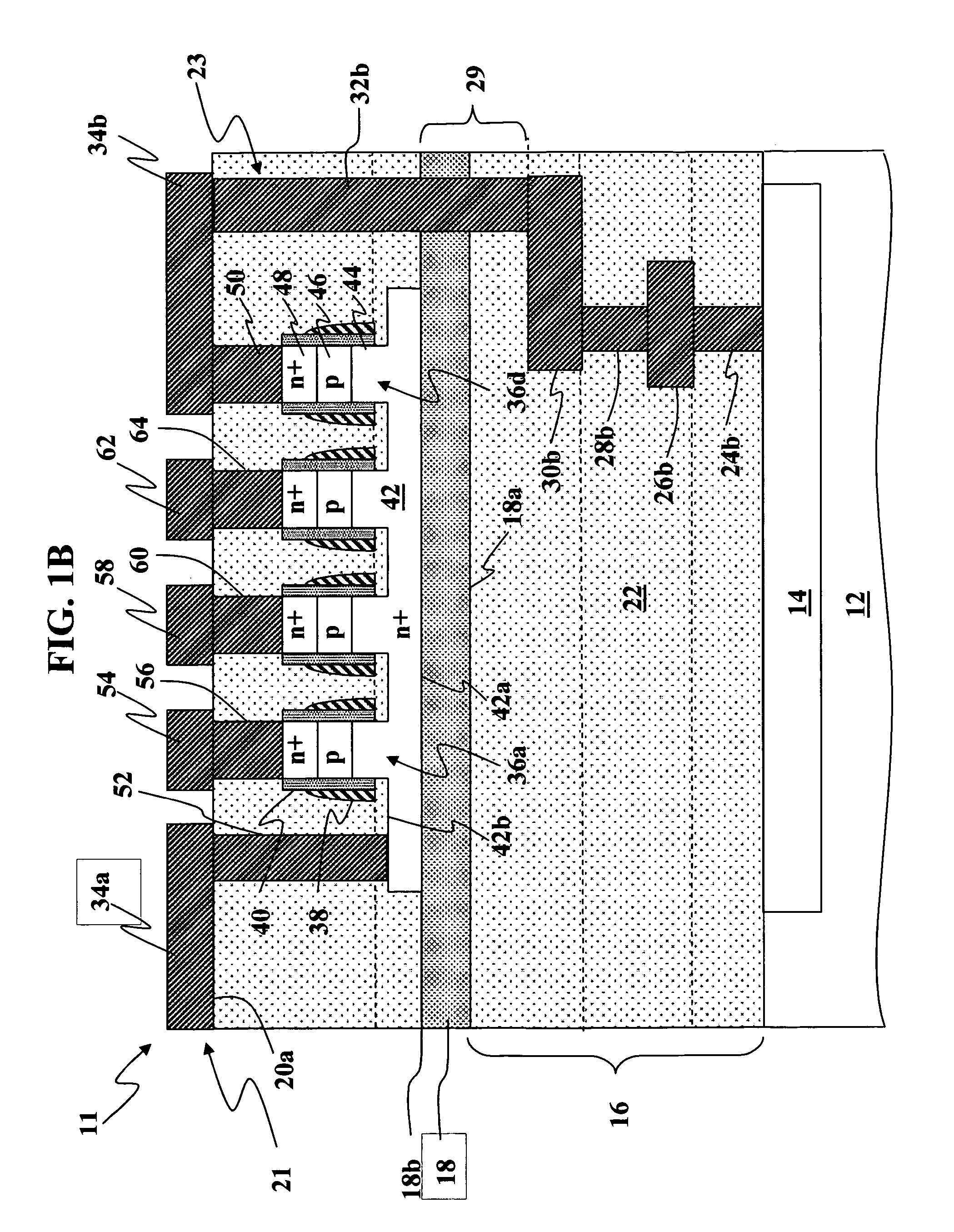
[0013]FIG. 1A is a simplified sectional view of a circuit 10 in accordance with the present invention. It should be noted that in the following figures, like reference characters indicate corresponding elements throughout the several views. Circuit 10 can be included in a number of different circuits. For example, it can be included in a processor chip or stand-alone memory. In this embodiment, circuit 10 includes electronic devices positioned above a microprocessor and / or control circuitry. As discussed in more detail below, the electronic devices are coupled to the microprocessor and / or control circuitry through conductive vias and / or interconnects.

[0014] In this embodiment, circuit 10 includes a substrate 12 which carries an electronic circuit 14. In this example, electronic circuit 14 is positioned adjacent to a surface 12a of substrate 12, but in other examples, circuit 14 can extend above or below surface 12a. Substrate 12 includes silicon, but it can include many other diffe...


PUM


Abstract

An apparatus includes a semiconductor chip with a base support structure having a surface and an opposed surface. At least one device structure extends from the surface of the base support structure. A first conductive region is coupled to the base support structure. At least a portion of the first conductive region extends below the opposed surface.

Description

CROSS REFERENCE TO RELATED APPLICATIONS [0001] This is a continuation-in-part of application Ser. No. 10 / 873,969, entitled “THREE-DIMENSIONAL INTEGRATED CIRCUIT STRUCTURE AND METHOD OF MAKING SAME”, which was filed 21 Jun. 2004 and is incorporated in its entirety herein by reference.BACKGROUND OF THE INVENTION [0002] 1. Field of the Invention [0003] This invention relates generally to semiconductor circuitry and, more particularly, to three dimensional vertical semiconductor devices. [0004] 2. Description of the Related Art [0005] Advances in semiconductor manufacturing and digital systems architecture have provided chips or integrated circuits with many millions of active and passive circuit components, along with the interconnects needed to create the desired circuit networks. As is well-known, most integrated circuits include transistors that are primarily implemented on a single major surface of a substrate, such as a semiconductor wafer. These laterally oriented devices consume...

Claims


Application Information

Patent Timeline
Patent Type & Authority Applications(United States)
IPC IPC(8): H01L21/20H01L21/30H01L21/336H01L21/46H01L21/58H01L23/48H01L27/108H01L27/148
CPCH01L21/2007H01L24/83H01L2924/1305H01L2924/1301H01L2924/1306H01L2924/01033H01L24/29H01L27/0688H01L27/11551H01L2224/291H01L2224/8385H01L2924/01005H01L2924/01013H01L2924/01015H01L2924/01018H01L2924/01027H01L2924/01029H01L2924/01038H01L2924/01047H01L2924/01049H01L2924/01056H01L2924/01073H01L2924/01074H01L2924/01075H01L2924/01078H01L2924/01079H01L2924/07802H01L2924/13091H01L2924/14H01L2924/1433H01L2924/19041H01L2924/19042H01L2924/19043H01L2924/30105H01L2924/3011H01L2924/00H01L2924/12036H01L23/48H10B41/20
Inventor LEE, SANG-YUN
Owner BESANG
Why Eureka
Try Eureka