Electroluminescence panel

a technology of electroluminescence and panel, applied in the field of electroluminescence, can solve the problems of increasing the dependence of display color on the viewing angle, degrading the organic layer, and increasing the degradation of the organic layer, so as to achieve the effect of improving the dependence of the viewing angl

Active Publication Date: 2005-12-22
SANYO ELECTRIC CO LTD
View PDF17 Cites 107 Cited by
  • Summary
  • Abstract
  • Description
  • Claims
  • Application Information

AI Technical Summary

Benefits of technology

[0016] As described, according to the present invention, each pixel has portions of differing cavity lengths, and therefore the viewing angle dependency can be improved.

Problems solved by technology

In the organic EL element, however, an organic layer is degraded with use, and in particular, there is a problem in that when the current to be applied through the organic layer is increased in order to increase the light emission luminance, degradation of the organic layer is accelerated.
When a microcavity is used, however, there is a problem in that a dependence of the display color on the viewing angle (viewing angle dependency) is increased.

Method used


Image

  • Electroluminescence panel
  • Electroluminescence panel
  • Electroluminescence panel

Examples


Embodiment Construction

[0029] Preferred embodiments of the present invention will now be described referring to the drawings.

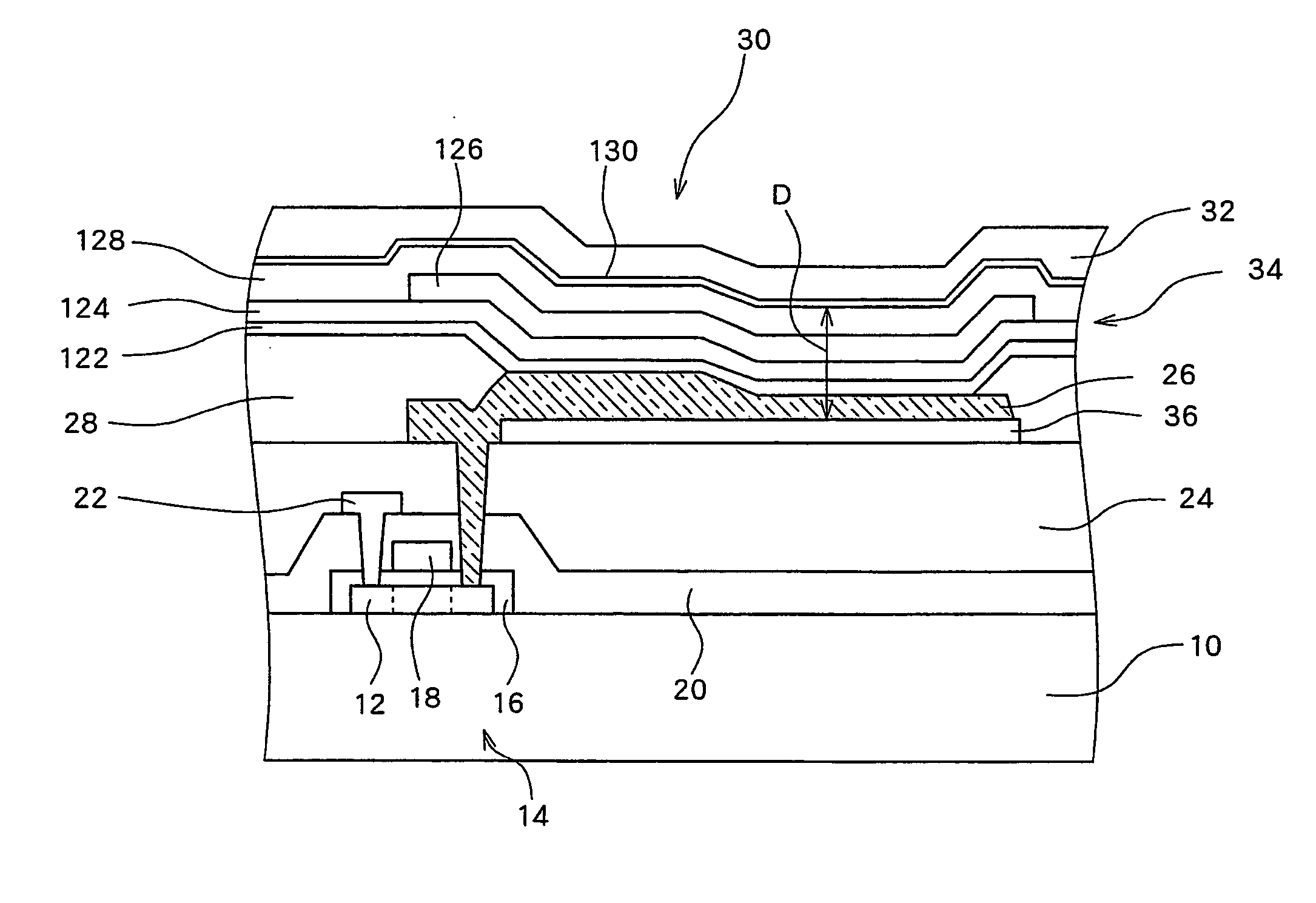
[0030]FIG. 1 is a schematic view showing a structure of a portion of a pixel forming a microcavity in a display panel according to a preferred embodiment of the present invention.

[0031] A semiconductor layer 12 is formed corresponding to a predetermined location of a glass substrate 10. The semiconductor layer 12 is used for a TFT, an electrode, or wiring. In the illustrated configuration, the semiconductor layer 12 forms a source region, a channel region, and a drain region of a driver TFT 14. The semiconductor layer 12 of the driver TFT 14 is covered with a gate insulating film 16 and a gate electrode 18 is formed above the gate insulating film 16 and above the channel region of the semiconductor layer 12. In addition, an interlayer insulating film 20 is formed over the entire surface covering the gate electrode 18 and the gate insulating film 16.

[0032] A source electrode 22 is...


PUM


Abstract

An electroluminescence panel having an electroluminescence element in each pixel, wherein the electroluminescence element comprises an emissive element layer having at least a light emitting function between a reflective film and a semi-transmissive film which is provided opposing the reflective film and have portions having different cavity lengths in one pixel, the cavity length being a distance between the reflective film and the semi-transmissive film. Such a structure can be realized, for example, by changing a thickness of a transparent electrode which is a lower electrode of the element. Because peak wavelength that can be intensified can be varied among regions in one pixel having different cavity lengths, a viewing angle dependency is improved.

Description

CROSS-REFERENCE TO RELATED APPLICATIONS [0001] The entire disclosure of Japanese Patent Application No. 2004-181850 including specification, claims, drawings, and abstract is incorporated herein by reference. BACKGROUND OF THE INVENTION [0002] 1. Field of the Invention [0003] The present invention relates to an electroluminescence (hereinafter simply referred to as “EL”) panel having an EL element in each pixel, and in particular to an EL panel having a micro-resonator (microcavity) in each pixel for intensifying light of a particular wavelength. [0004] 2. Description of the Related Art [0005] Recently, flat panel displays (FPD) having thin thickness and a size which can be reduced have attracted much attention. A liquid crystal display device which is a well known example of the FPD is already used in various devices. In addition, much research and development are dedicated to light emitting devices (such as a display device and a light source) which use a self-emissive EL element,...

Claims


Application Information

Patent Timeline
Patent Type & Authority Applications(United States)
IPC IPC(8): H01L51/52H05B33/00
CPCH01L51/5265H10K50/852H01L2924/12044H10K59/35H10K59/123H10K50/11H10K50/80H10K50/805H10K50/85
Inventor OMURA, TETSUJINISHIKAWA, RYUJI
Owner SANYO ELECTRIC CO LTD
Why Eureka
Try Eureka