Semiconductor integrated circuit, drive circuit, and plasma display apparatus

Inactive Publication Date: 2005-12-29
FUJITSU HITACHI PLASMA DISPLAY LTD
View PDF5 Cites 12 Cited by
  • Summary
  • Abstract
  • Description
  • Claims
  • Application Information

AI Technical Summary

Benefits of technology

[0027] Similarly, in the semiconductor integrated circuit according to the second aspect of the present invention, the first semiconductor chip having the input terminal and the light emitting device and the second semiconductor chip having the light receiving device and the amplifier circuit are contained in a single package and the second semiconductor chip comprises a delay time adjustment circuit capable of delaying the rising edge or the falling edge of an electric signal obtained from the light receiving element to adjust a delay time and, therefore, the total delay time can be adjusted to a predetermined value despite the variations in the delay time of each device and circuit and the temperature characteristic of the delay time of each device and circuit can be t

Problems solved by technology

Because of this, even if the optimum phase adjustment is done at a specific temperature, there may occur deviation in the phase adjustment under other temperature conditions due to the difference in ambient temperature.
Also, when the pre-drive circuit that utilizes the above-mentioned optical transmission circuit is used in the sustain circuit in the p

Method used


Image

  • Semiconductor integrated circuit, drive circuit, and plasma display apparatus
  • Semiconductor integrated circuit, drive circuit, and plasma display apparatus
  • Semiconductor integrated circuit, drive circuit, and plasma display apparatus

Examples


first embodiment

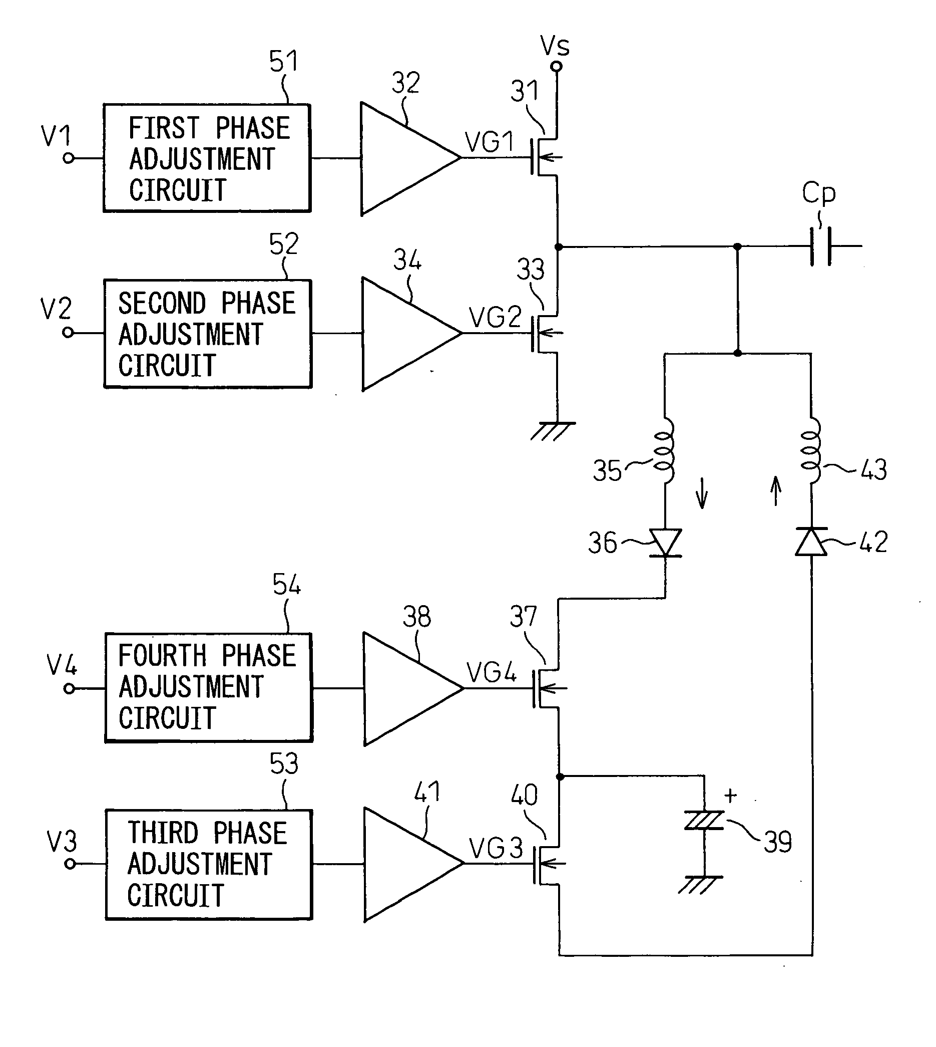
[0062]FIG. 4 is a general block diagram of a PDP apparatus in the present invention. In a PDP 10, n first (X) electrodes and n second (Y) electrodes 12 are arranged adjacently by turns to form n pairs of X electrode 11 and Y electrode 12, and a discharge is caused to occur between the X electrode 11 and the Y electrode 12 of each pair to emit light to provide a display. The Y electrode and the X electrode are referred to as the display electrode, or the sustain electrode in some cases. Address electrodes 13 are provided in the direction perpendicular to the direction in which the display electrodes extend and a display cell is formed at the intersection of the X electrode 11 and the Y electrode 12.

[0063] The Y electrodes 12 are connected to a scan driver 14. The scan drive 14 is provided with switches 16, the number of which being equal to that of Y electrodes, and during the address period, the switches 16 are switched over so that a scan pulse from a scan signal generation circuit...

fourth embodiment

[0101]FIG. 19 is a block diagram showing the general configuration of a PDP apparatus in the present invention. The PDP apparatus is required to be highly precise and U.S. Pat. No. 6,373, 452 discloses a system in which light is emitted between display electrodes to produce a display. This system is referred to as the ALIS system and the same term is used here. The detailed configuration of the ALIS system is disclosed in U.S. Pat. No. 6,373,452, therefore, only the points relating to the present invention are briefly explained below.

[0102] As shown in FIG. 19, in a PDP employing the ALIS system, n Y electrodes (second electrodes) 12-0 and 12-E and n+1 X electrodes (first electrodes) 11-0 and 11-E are arranged adjacently by turns and light emission to produce a display is carried out between every pair of neighboring display electrodes (Y electrode and X electrode). Therefore, 2n display lines are formed with 2n+1 display electrodes. In other words, in the ALIS system, it is possibl...

fifth embodiment

[0111] The delay time adjustment circuit 61 in the fifth embodiment is constituted of the resistor R10 and resistors RI1, RI2, and RI3, a capacitor C1, and transistors QI1, QI2, and QI3. The input / output delay time comparison circuit 68 is constituted of a resistor RI4, a capacitor CI4, a reference voltage source Vref, and a differential amplifier circuit MI2. The output pulse detection circuit 66 is constituted of a differential amplifier circuit MI1.

[0112] The operation of the IC in the fifth embodiment is described below. In FIG. 24, the output pulse detection circuit 66 detects an output voltage output from OUT1 and converts the output voltage into an output pulse detection signal VO1 on the basis of GND, as shown in FIG. 25 (F). The input / output delay time detection circuit 67 detects the difference between the front edge of the output pulse detection signal VO1 and the front edge of the input signal IN1 and outputs an input / output delay time detection pulse VIO1 showing the ti...


PUM


Abstract

A semiconductor integrated circuit capable of reducing the influence of the difference in ambient temperature etc. and realizing a stable phase adjustment circuit has been disclosed. The semiconductor integrated circuit comprises a delay time adjustment circuit for delaying the rising edge or the falling edge of an input signal and changing the amount of delay, a comparison circuit for comparing an output signal from the delay time adjustment circuit with a predetermined voltage, a high-level shift circuit for shifting an output signal from the comparison circuit into a signal on the basis of an output reference voltage, and an output amplifier circuit for amplifying an output signal from the high-level shift circuit and outputting a signal for driving the semiconductor device, wherein the delay time adjustment circuit, the comparison circuit, the high-level shift circuit, and the output amplifier circuit are formed on a single chip.

Description

CROSS REFERENCE TO RELATED APPLICATION [0001] This application is based upon and claims the benefit of priority from the prior Japanese Patent Applications No. 2004-189766, filed on Jun. 28, 2003 and No. 2004-353595, filed on Dec. 7, 2004, the entire contents of which are incorporated herein by reference. BACKGROUND OF THE INVENTION [0002] The present invention relates to a semiconductor integrated circuit used in a sustain circuit of a plasma display apparatus, to a drive circuit, and to a plasma display apparatus using these circuits. [0003] The plasma display panel (PDP) is a self-emitting-type display has excellent visibility, is thin, and is capable of producing a large display at a high speed. Therefore, it is attracting interest as a display panel and as a replacement for a CRT. As the basic configuration of a PDP is disclosed in, for example, EP 1139323A, a detailed description is not give here but only points that directly relate to the present invention are described below...

Claims


Application Information

Patent Timeline
IPC IPC(8): G09G3/20G09G3/288G09G3/291G09G3/294G09G3/296G09G3/298G09G3/299H03K5/13H03K17/14H03K17/687H03K17/78H03K19/0185
CPCG09G3/2965G09G3/299G09G2300/0408G09G2330/024G09G2310/0289G09G2320/041G09G2310/0267G09G3/296
Inventor ONOZAWA, MAKOTOKISHI, TOMOKATSUOKADA, YOSHINORIHIRA, MASATOSHI
Owner FUJITSU HITACHI PLASMA DISPLAY LTD
Why Eureka
Try Eureka