Light emitting display and driving method thereof

Active Publication Date: 2005-12-29
SAMSUNG DISPLAY CO LTD
View PDF8 Cites 295 Cited by
  • Summary
  • Abstract
  • Description
  • Claims
  • Application Information

AI Technical Summary

Benefits of technology

[0023] The at least one of the pixel circuits may further include a third switch being turned on in response to a third level of the select signal for transmitting the data signal to a second main electrode of the first transistor, and a fourth switch being t

Problems solved by technology

In contrast, when a low data voltage VDATA is applied to the gate electrode of the driving transistor DM, the gate-source voltage VGS of the driving transistor DM is raised at which point a large amount of current IOLED is applied to the pixel electrode, resulting

Method used


Image

  • Light emitting display and driving method thereof
  • Light emitting display and driving method thereof
  • Light emitting display and driving method thereof

Examples


Embodiment Construction

[0043] In the following detailed description, only certain exemplary embodiments of the present invention are shown and described, simply by way of illustration. As those skilled in the art would realize, the described embodiments may be modified in various different ways, all without departing from the spirit or scope of the present invention.

[0044] Accordingly, the drawings and description are to be regarded as illustrative in nature, and not restrictive. There may be parts shown in the drawings, or parts not shown in the drawings, that are not discussed in the specification as they are not essential to a complete understanding of the invention. Like reference numerals designate like elements. The phrases such as “one thing is coupled to another” may denote either “a first one is directly coupled to a second one” or “the first one is electrically coupled to the second one with a third one provided between”.

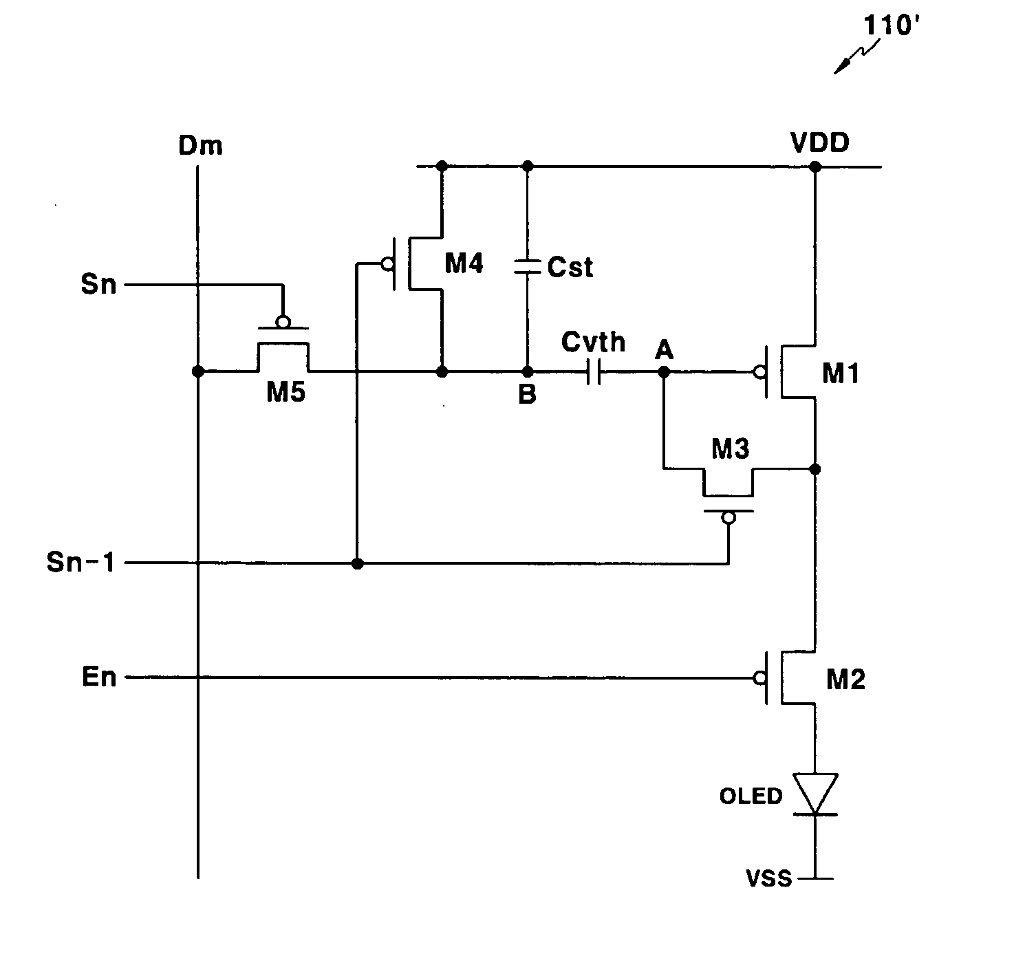
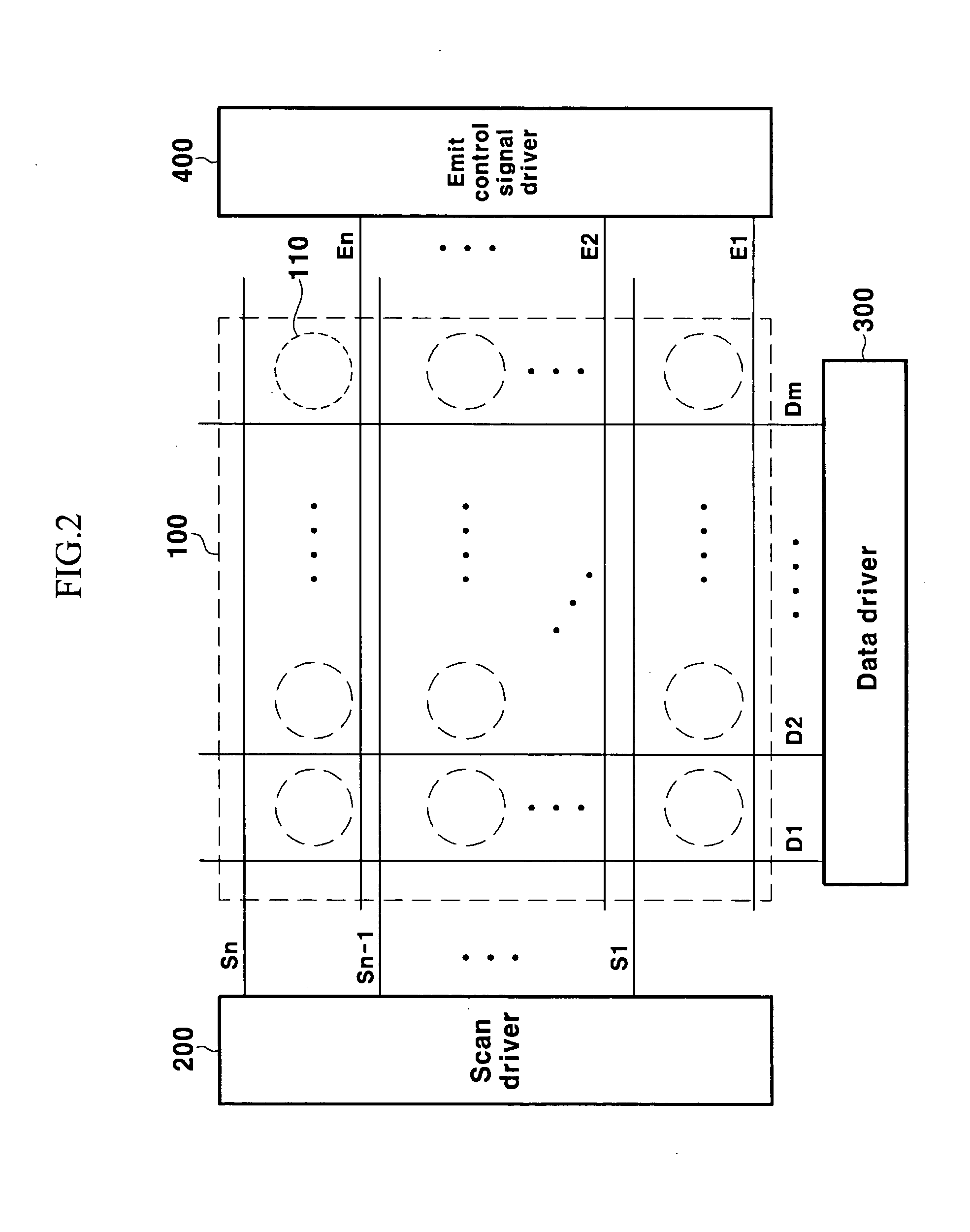
[0045]FIG. 2 is a schematic view illustrating an OLED display according t...


PUM


Abstract

A light emitting display includes pixel circuits capable of compensating for the threshold voltages of their driving transistors. Each pixel circuit includes a driving transistor, a capacitor having one end coupled to a gate electrode of the driving transistor, a first switch coupled between the gate electrode of the driving transistor and a first main electrode, which is turned on in response to a first level of a first control signal for diode-coupling the driving transistor, and a second switch turned on in response to a second level of a second control signal to transmit current flowing out of the first main electrode of the driving transistor to a light emitting element. The second switch is turned on when the first switch is turned on for a first period longer than 0.05 μs and shorter than 2.5 μs. The second switch is turned on when the first switch is turned off.

Description

CROSS REFERENCE TO RELATED APPLICATION [0001] This application claims priority to and the benefit of Korean Patent Application No. 10-2004-0049301 filed on Jun. 29, 2004 in the Korean Intellectual Property Office, the entire content of which is incorporated herein by reference. BACKGROUND OF THE INVENTION [0002] (a) Field of the Invention [0003] The present invention relates to a light emitting display, and more particularly to a method of compensating for the variance in the threshold voltage of the driving transistor among the pixel circuits of the light emitting display. [0004] (b) Description of the Related Art [0005] In general, an organic light emitting diode (OLED) display, which is a light emitting display for displaying images using the electroluminescence of an organic material, displays images by driving N×M organic light emission cells arranged in a matrix on a voltage basis or a current basis. [0006] An organic light emission cell, which is also called an organic light ...

Claims


Application Information

Patent Timeline
IPC IPC(8): G09G3/30G09G3/32H05B44/00
CPCG09G3/3233G09G2300/0819G09G2300/0842G09G2320/043G09G2300/0861G09G2310/0251G09G2300/0852G09G3/30
Inventor EOM, KI-MYEONGOH, CHOON-YUL
Owner SAMSUNG DISPLAY CO LTD
Why Eureka
Try Eureka