
Wide bandgap HEMTs with source connected field plates

Active Publication Date: 2006-01-12
CREE INC
View PDF34 Cites 73 Cited by
  • Summary
  • Abstract
  • Description
  • Claims
  • Application Information

AI Technical Summary

Benefits of technology

[0011] The present invention provides transistors with a field plate connected to the source electrode, with typical transistors utilizing the invention being HEMTs. One embodiment of a HEMT according to the present invention comprises a plurality of active semiconductor layers formed on a substrate with a two dimensional electron gas (2DEG) at the heterointerface between two of said plurality of active layers. Source and drain electrodes are formed in contact with the 2DEG and a

Problems solved by technology

Electron trapping and the resulting difference between DC and RF characteristics have been a limiting factor in the performance of these devices.
However, due to the high electric fields existing in these structures, charge trapping is still an issue.
This can result in a significant FP-to-drain capacitance and the field plate being connected to the gate adds additional gate-to-drain capacitance (Cgd) to the device.
This can not only reduce gain, but can also cause instability due to poorer input-output isolation.

Method used


Image

  • Wide bandgap HEMTs with source connected field plates
  • Wide bandgap HEMTs with source connected field plates
  • Wide bandgap HEMTs with source connected field plates

Examples


Embodiment Construction

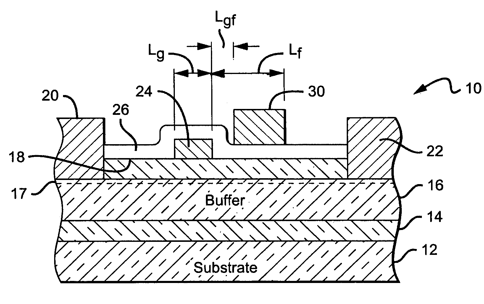
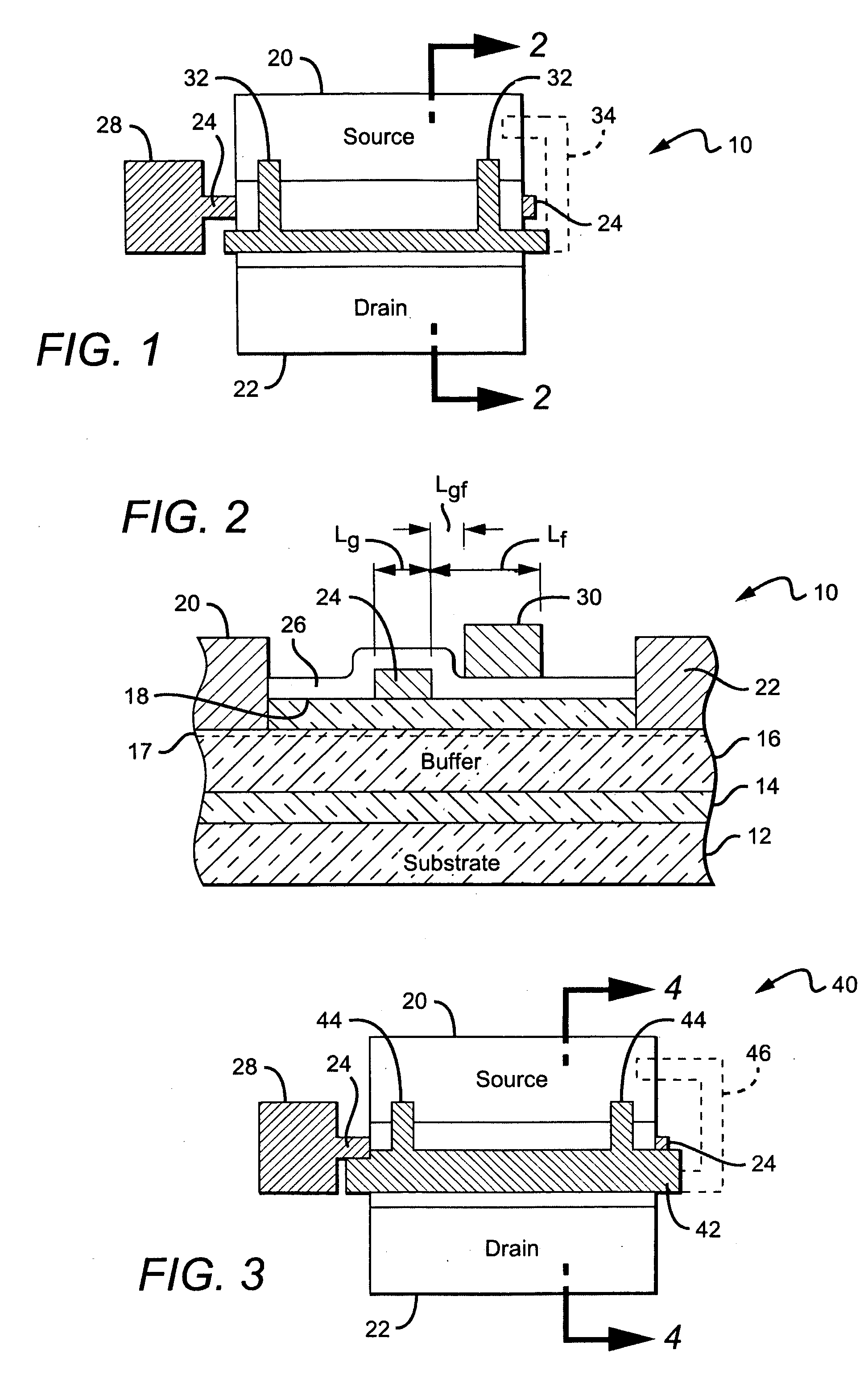
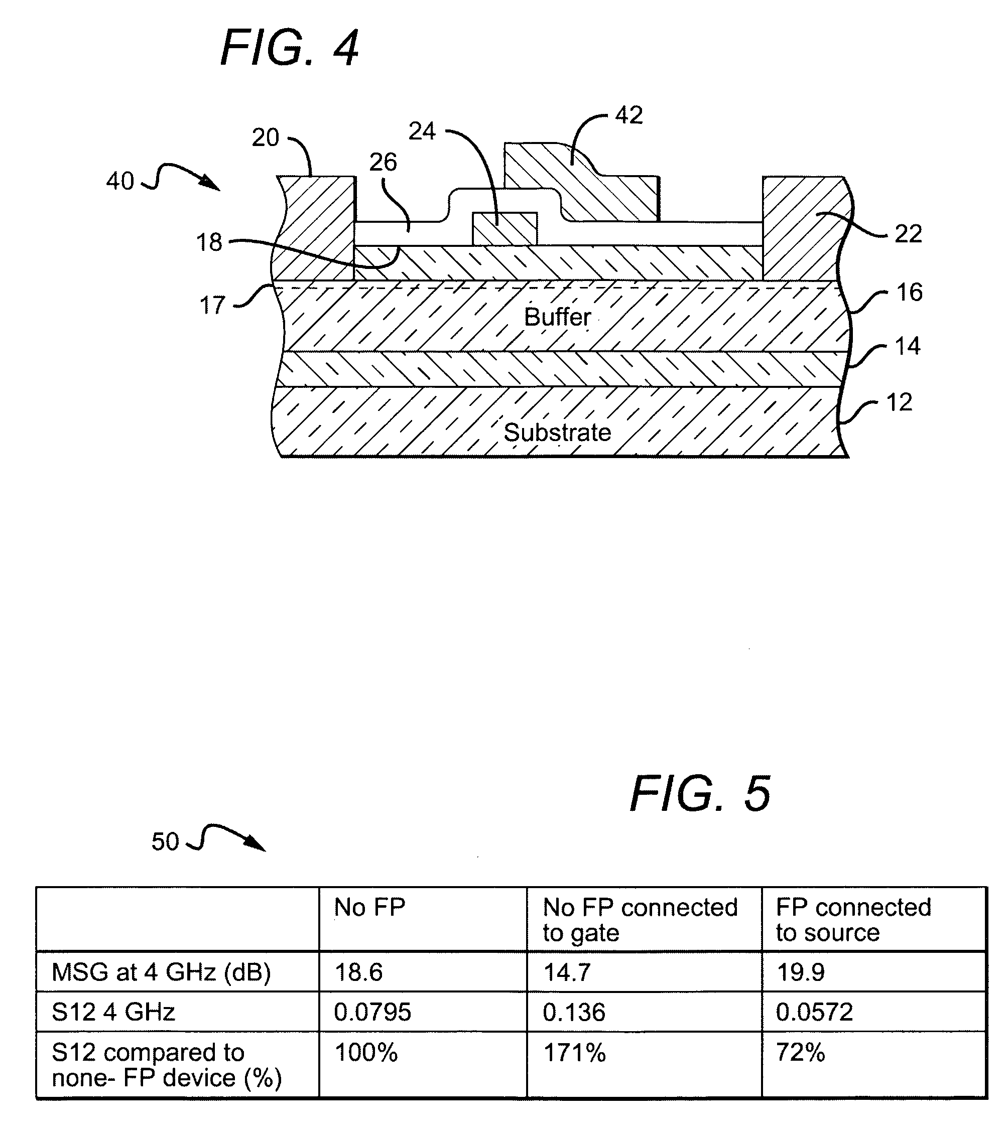
[0024] The field plate arrangements according to the present invention can be used with many different transistor structures. Wide bandgap transistor structures generally include an active region, with metal source and drain electrodes formed in electrical contact with the active region, and a gate electrode formed between the source and drain electrodes for modulating electric fields within the active region. A spacer layer is formed above the active region. The spacer layer can comprise a dielectric layer, or a combination of multiple dielectric layers. A conductive field plate is formed above the spacer layer and extends a distance Lf from the edge of the gate electrode toward the drain electrode.

[0025] The field plate can be electrically connected to the source electrode. This field plate arrangement can reduce the peak electric field in the device, resulting in increased breakdown voltage and reduced trapping. The reduction of the electric field can also yield other benefits s...


PUM


Abstract

A HEMT comprising a plurality of active semiconductor layers formed on a substrate. Source electrode, drain electrode, and gate are formed in electrical contact with the plurality of active layers. A spacer layer is formed on at least a portion of a surface of said plurality of active layers and covering the gate. A field plate is formed on the spacer layer and electrically connected to the source electrode, wherein the field plate reduces the peak operating electric field in the HEMT.

Description

[0001] This application claims the benefit of provisional application Ser. No. 60 / 570,519 to Wu et al., which was filed on May 11, 2004.[0002] This invention was made with Government support under ONR / DARPA Government Contract No. N00014-02-0306. The Government has certain rights in this invention.BACKGROUND OF THE INVENTION [0003] 1. Field of the Invention [0004] The present invention relates to transistors and particularly to transistors utilizing field plates. [0005] 2. Description of the Related Art [0006] Improvements in the manufacturing of AlGaN / GaN semiconductor materials have helped advance the development of AlGaN / GaN transistors, such as high electron mobility transistors (HEMTs) for high frequency, high temperature and high power applications. AlGaN / GaN has large bandgaps, high peak and saturation electron velocity values [B. Gelmont, K. Kim and M. Shur, Monte Carlo Simulation of Electron Transport in Gallium Nitride, J. Appl. Phys. 74, (1993), pp. 1818-1821]. AlGaN / GaN ...

Claims


Application Information

Patent Timeline
IPC IPC(8): H01L29/739H01L29/06H01L29/20H01L29/40H01L29/778
CPCH01L29/2003H01L29/7787H01L29/402H01L29/41725H01L29/42316H01L29/66462
Inventor WU, YIFENGPARIKH, PRIMITMISHRA, UMESHMOORE, MARCIA
Owner CREE INC
Learn More