Pixel defect detecting/correcting device and pixel defect detecting/correcting method

a technology of pixel defect and detecting device, which is applied in the field of pixel defect detecting and correcting apparatus, and pixel defect detecting and correcting method, which can solve the problems of increasing the capacity of memory and the enlarged gate scale of the detection circui

Inactive Publication Date: 2006-01-19
SONY CORP
View PDF6 Cites 41 Cited by
  • Summary
  • Abstract
  • Description
  • Claims
  • Application Information

AI Technical Summary

Benefits of technology

[0018] Accordingly, the present invention is made in light of the above-described points and provides a pixel defect detecting and correcting apparatus and a pixel defect detecting and correcting method, in which the number of correctable defect pixels is not restricted to the capacity of a memory device, and further defects subsequently occurred and not detected at the time of adjustment due to a change in operative temperature or the like can be detected and corrected sufficiently.

Problems solved by technology

However, in the above-described conventional defect pixel correcting method, the number of defect pixels that are correctable is restricted to the capacity of a memory device, so that in order to increase the number of pixels to be corrected, it is necessary to increase the capacity of the memory device, causing a gate scale of a detection circuit to be enlarged, which is an inconvenience.
Further, defects later occurred and not detected at the time of adjustment due to a change in operative temperature or the like cannot be detected and corrected sufficiently in conventional methods, which is an inconvenience.
Further, in Patent Literature 2, since the level difference between a first pixel and a second pixel in the vicinity of the first pixel in an imaging device is detected and the result of a judgment with respect to defect pixels as compared with a threshold value is stored in a memory in advance, the number of correctable defect pixels is restricted to the capacity of the memory, and in order to increase the number of correctable pixels, it is necessary to increase the capacity of the memory, which is an inconvenience.

Method used


Image

  • Pixel defect detecting/correcting device and pixel defect detecting/correcting method
  • Pixel defect detecting/correcting device and pixel defect detecting/correcting method
  • Pixel defect detecting/correcting device and pixel defect detecting/correcting method

Examples


Embodiment Construction

[0029] Hereinafter, an embodiment of the present invention will be explained, referring to the drawings as need arises.

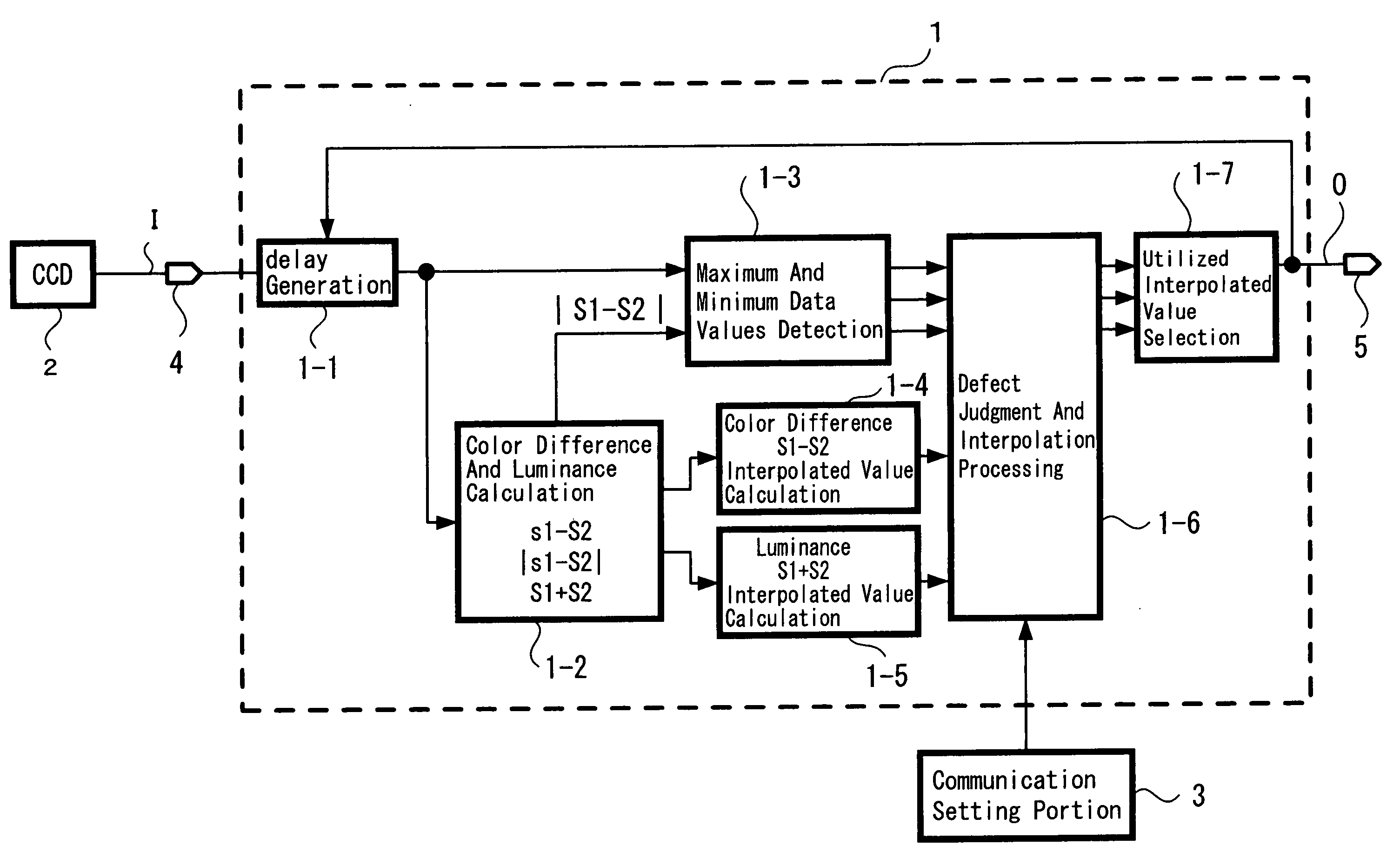
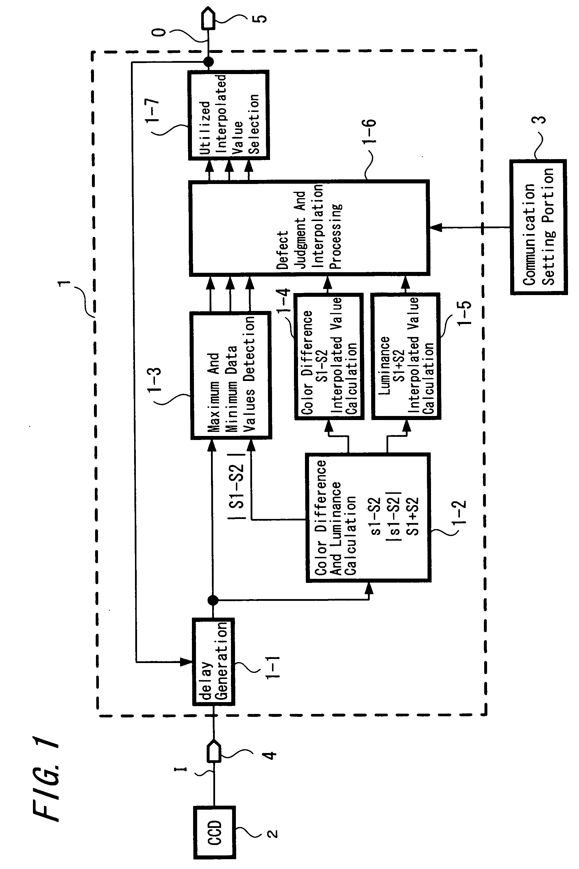
[0030]FIG. 1 schematically shows in a simple manner a basic configuration of a defect detection and correction controlling block applied to an embodiment of the present invention.

[0031] First, the configuration of a defect detection and correction controlling block 1 applied to this embodiment is explained. The pixel defect detection and correction controlling block 1, which functions as the core of this embodiment, is positioned between an imaging block having a CCD 2 or the like supplying through an input terminal 4 an image input signal I including pixel defects and a camera signal processing block generating a luminance signal and a color signal which supply an image output signal O including data corrected through an output terminal 5.

[0032] The defect detection and correction controlling block 1 applied to this embodiment includes a color difference and lum...


PUM


Abstract

A pixel defect detecting and correcting apparatus according to the present invention is provided in which the number of correctable defect pixels is not restricted to the capacity of a memory device and defects subsequently generated can be detected and corrected; and includes a color difference and luminance calculating block 1-2 which calculates the absolute values of the color differences of adjacent pixels and a defect judgment target pixel, and color difference and luminance data; a maximum and minimum data values detecting block 1-3 which detects the maximum and minimum values of various kinds of data based on values calculated from the color difference and luminance; a color difference interpolated value calculating block 1-4 and a luminance interpolated value calculating block 1-5 which obtain the color difference interpolated values and luminance interpolated values of the defect judgment target pixel, respectively; and a defect judgment and interpolation processing block (1-6) which, using a plurality of defect detecting methods, concurrently performs defect judgment of the defect judgment target pixel with respect to each of the defect detecting method and executes interpolation processing according to the defect detecting methods in the case of pixel defects; and an interpolated value for use selecting block (1-7) which selects the final output values of pixels judged to be defective.

Description

TECHNICAL FIELD [0001] The present invention relates to a pixel defect detecting and correcting apparatus, and a pixel defect detecting and correcting method, for example. BACKGROUND ART [0002] As pixel defects in a solid-state imaging device, there are a white defect in which a certain amount of electric charge is invariably added to a normal signal (derived from a crystalline defect or the like in a CCD (Charge Coupled Device)), and a black defect in which either a signal level decreases at a certain ratio (derived from scratches on on-chip lenses or the like of a CCD) or a signal level that is 0 or below is invariably output (derived from the opening of a photodiode of a CCD) with respect to a normal signal. These pixel defects become dot-like blemishes at the time of imaging and cause deterioration in image quality, so that various means for detecting and correcting defects by signal processing have been proposed. [0003] With respect to pixel defect detecting and correcting appa...

Claims


Application Information

Patent Timeline
Patent Type & Authority Applications(United States)
IPC IPC(8): H04N9/64H01L27/14H04N5/335H04N5/367H04N5/372H04N9/04H04N9/07
CPCH04N9/045H04N5/3675H04N25/683H04N23/843H04N25/68H04N23/12
Inventor YONEDA, YUTAKAKOISO, MANABU
Owner SONY CORP
Why Eureka
Try Eureka