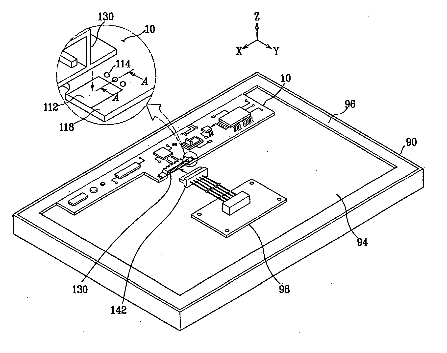
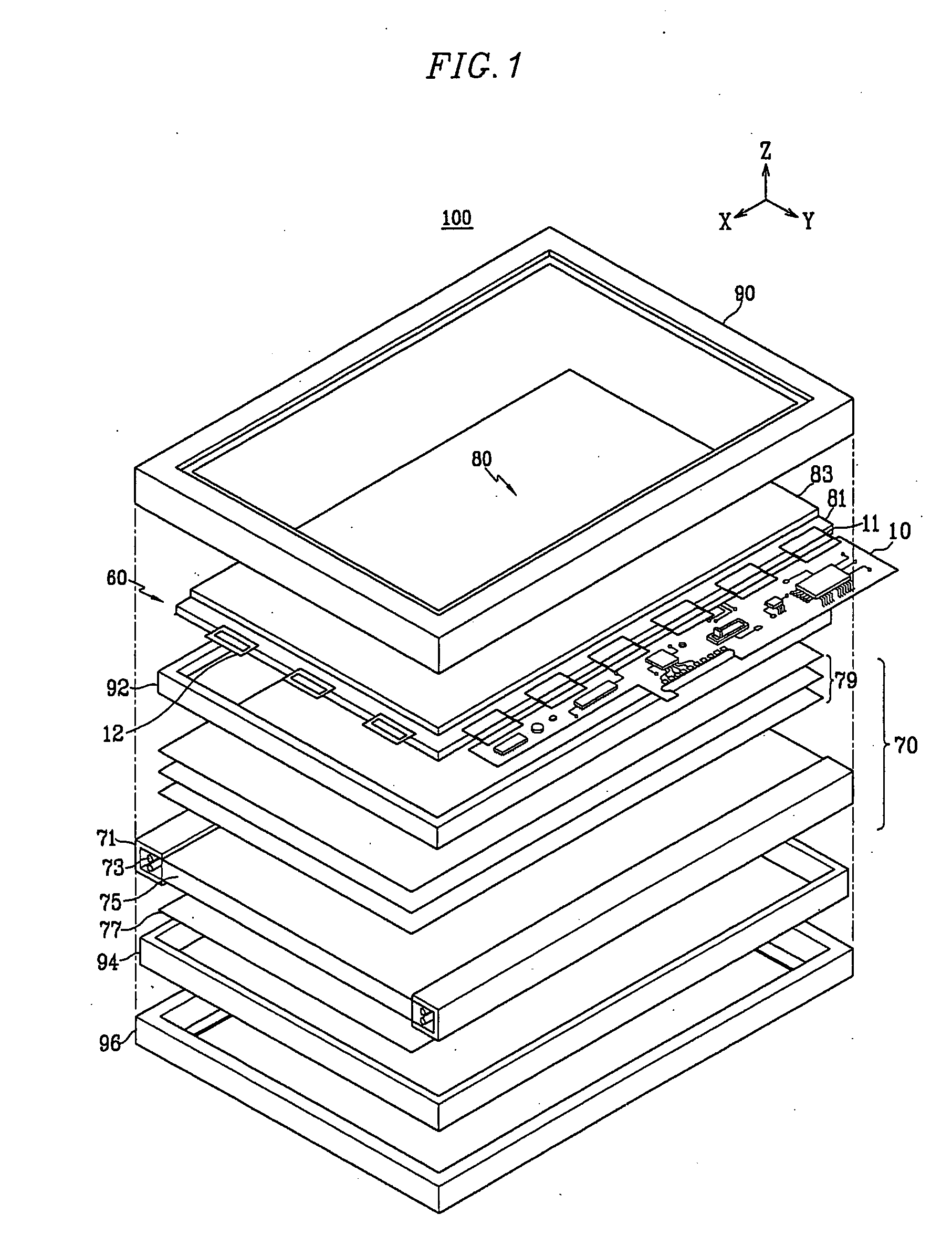
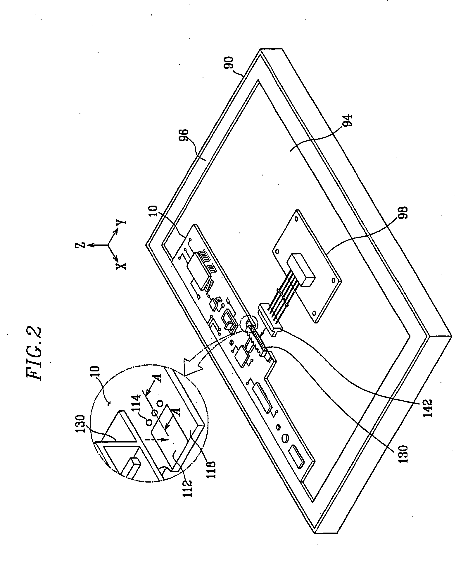
Printed circuit board and display device using the same
- Summary
- Abstract
- Description
- Claims
- Application Information
AI Technical Summary
Benefits of technology
Problems solved by technology
Method used
Image

Examples
experimental examples
[0068] Exfoliation intensity of both ends of a connector soldered to a connecting pad portion of a PCB is measured using a push-pull gauge (product by AIKOH Engineering; Model No. 1605 HTP). The push-pull gauge used in the present invention can measure exfoliation intensity in a range of about 0 to 50 kgf, and a speed thereof can be varied in a range of about 1 to 200 mm / min. Since exfoliation occurs when both ends of the connector are continuously pulled with increasing force, the exfoliation intensity is measured by calculating a peak value at a moment of exfoliation. Such a method for measuring exfoliation intensity is easily understood by those skilled in the art of the present invention, and thus a detailed explanation thereof is omitted.
[0069] EXPERIMENTAL EXAMPLES OF THE PRESENT INVENTION
[0070] In the present invention, like the PCB according to the exemplary embodiment of the present invention shown in FIG. 3, an experiment is executed by using a connector soldered to a co...
PUM
 Abstract
Description
Claims
Application Information
 - R&D Engineer
- R&D Manager
- IP Professional
- Industry Leading Data Capabilities
- Powerful AI technology
- Patent DNA Extraction
Browse by: Latest US Patents, China's latest patents, Technical Efficacy Thesaurus, Application Domain, Technology Topic.
© 2024 PatSnap. All rights reserved.Legal|Privacy policy|Modern Slavery Act Transparency Statement|Sitemap