Plasma processing apparatus and impedance adjustment method

Inactive Publication Date: 2006-02-02
TOKYO ELECTRON LTD
View PDF2 Cites 34 Cited by
  • Summary
  • Abstract
  • Description
  • Claims
  • Application Information

AI Technical Summary

Benefits of technology

[0015] In accordance with the present invention, there are provided a resonance circuit, a variable impedance unit installed on a power feed line of a first electrode and a detector for detecting an apparatus state to search a resonance point of the resonance circuit. In a state where plasma is generated, a signal of the apparatus state of the detector is detected while varying a value of the variable impedance unit, thereby searching a resonance point of the resonance circuit. Also, by adjusting an impedance on the side of the plasma source while setting a value of the variable impedance unit at the resonance point to a reference value, it is possible to minimize an impedance difference on the side of the plasma source between apparatuses or cleaning cycles due to dimensional tolerances or attachment errors of parts. Furthermore, since the adjustment can be performed in a state where the plasma is generated, a high impedance adjusting accuracy can be achieved. Moreover, since neither special measuring de

Problems solved by technology

In such a plasma processing apparatus, there is given rise on the side of a plasma source to a minor difference in the impedance between apparatuses or cleaning cycles due to dimensional tolerances or attachment errors of parts.
However, the c

Method used


Image

  • Plasma processing apparatus and impedance adjustment method
  • Plasma processing apparatus and impedance adjustment method
  • Plasma processing apparatus and impedance adjustment method

Examples


Embodiment Construction

[0030] Hereinafter, preferred embodiments of the present invention will be described in detail with reference to the accompanying drawings.

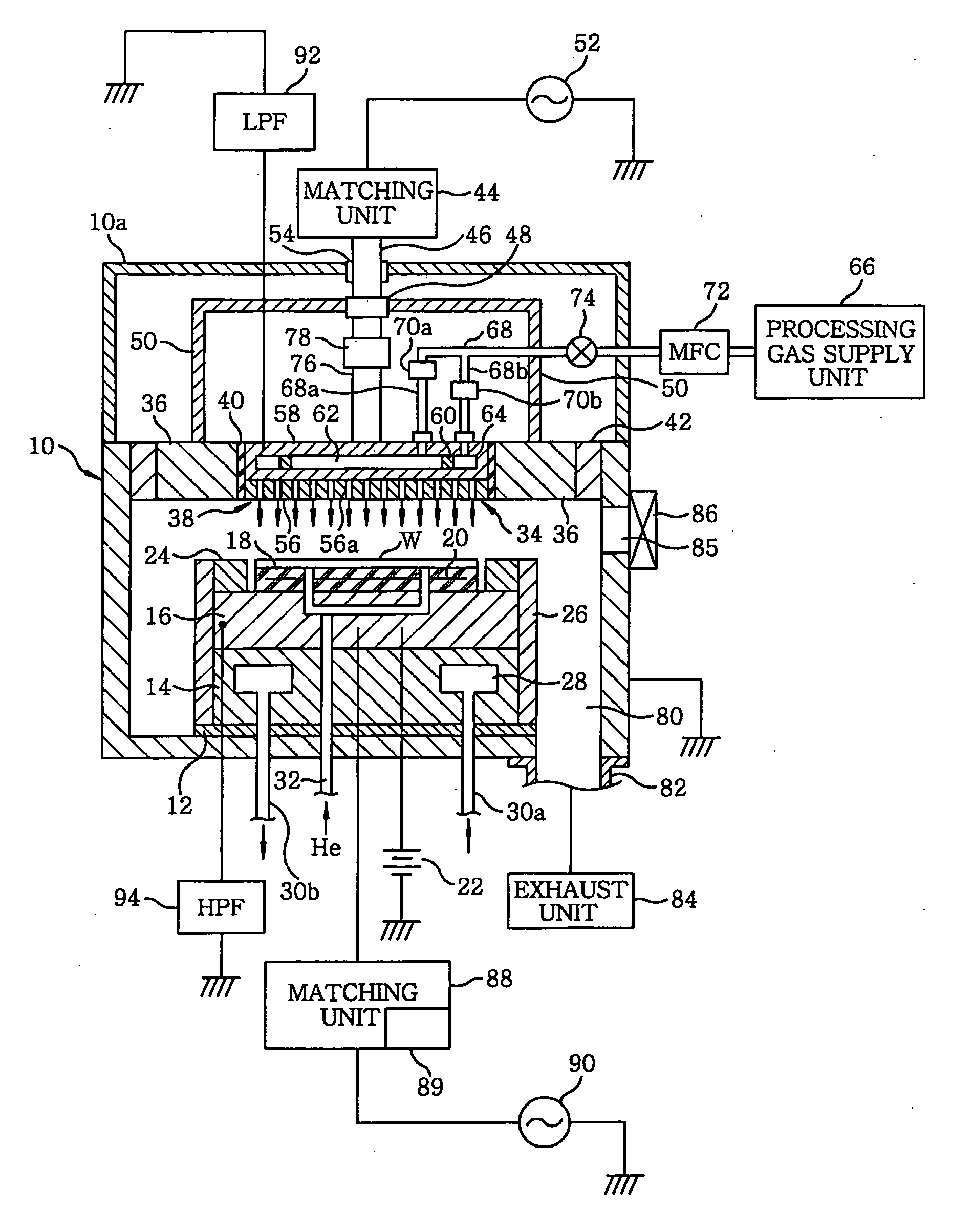
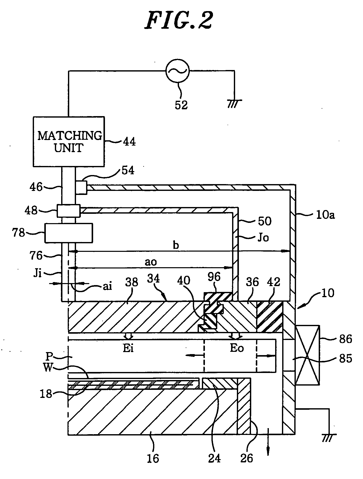
[0031]FIG. 1 is a schematic cross sectional view of a plasma etching apparatus in accordance with a preferred embodiment of the present invention.

[0032] The plasma etching apparatus is a capacitively coupled parallel flat type plasma etching apparatus having an approximately cylindrical chamber (processing vessel) 10 made of aluminum whose surface is treated by an anodic oxidization. The chamber 10 is frame grounded.

[0033] A columnar susceptor support 14 is provided on a bottom of the chamber 10 via an insulating plate 12 made of ceramic or the like. Further, a susceptor 16 made of, e.g., aluminum is installed on the susceptor support 14. The susceptor 16 forms a lower electrode, and a semiconductor wafer W as a substrate to be processed is mounted thereon.

[0034] Provided on top of the susceptor 16 is an electrostatic chuck 18 for adsorptivel...


PUM

PropertyMeasurementUnit
Currentaaaaaaaaaa
Frequencyaaaaaaaaaa
Capacitanceaaaaaaaaaa

Abstract

A plasma processing apparatus, for performing a plasma processing on a substrate to be processed by generating a plasma of the processing gas in an evacuable processing chamber, includes an impedance adjusting mechanism. The impedance adjusting mechanism is provided with a resonance circuit formed to allow a radio frequency current to flow into the first electrode; a variable impedance unit installed on a power feed line to the first electrode; a detector for detecting an apparatus state to be used to search a resonance point of the resonance circuit; and a controller for searching a resonance point of the resonance circuit by detecting a signal of the apparatus state of the detector while varying a value of the variable impedance unit in a state where the plasma is formed and then adjusting the value of the variable impedance unit at the resonance point to a reference value.

Description

FIELD OF THE INVENTION [0001] The present invention relates to a plasma processing apparatus for performing a plasma processing on a substrate such as a semiconductor substrate or the like and an impedance adjustment method employed in a plasma processing apparatus. BACKGROUND OF THE INVENTION [0002] For example, in a semiconductor device manufacturing process, a plasma processing such as an etching, a sputtering, a chemical vapor deposition (CVD) or the like is performed on a semiconductor wafer as a substrate to be processed. [0003] As for a plasma processing apparatus for performing such plasma processing, there are used many different kinds of processing apparatuses and a capacitively coupled parallel flat type plasma apparatus is a typical one most commonly used among them. [0004] In the capacitively coupled parallel flat type plasma processing apparatus, a pair of parallel flat electrodes (an upper and a lower electrode) is provided in a chamber, and a processing gas is introd...

Claims


Application Information

Patent Timeline
IPC IPC(8): C23C16/00
CPCH01J37/32174H01J37/32082
Inventor HIRANO, TAICHI
Owner TOKYO ELECTRON LTD
Why Eureka
Try Eureka