Resistor circuit
- Summary
- Abstract
- Description
- Claims
- Application Information
AI Technical Summary
Benefits of technology
Problems solved by technology
Method used
Image
Examples
Embodiment Construction
[0024] Hereinafter, description will be made of an embodiment of the present invention with reference to the drawings.
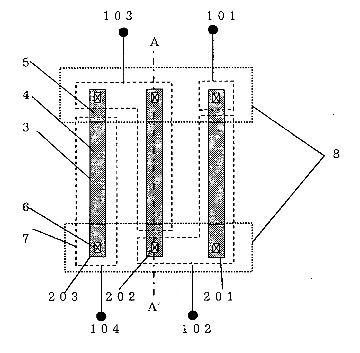
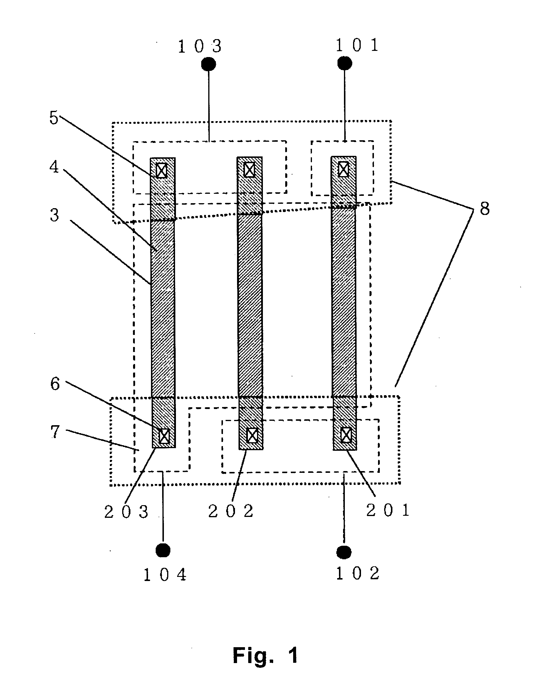
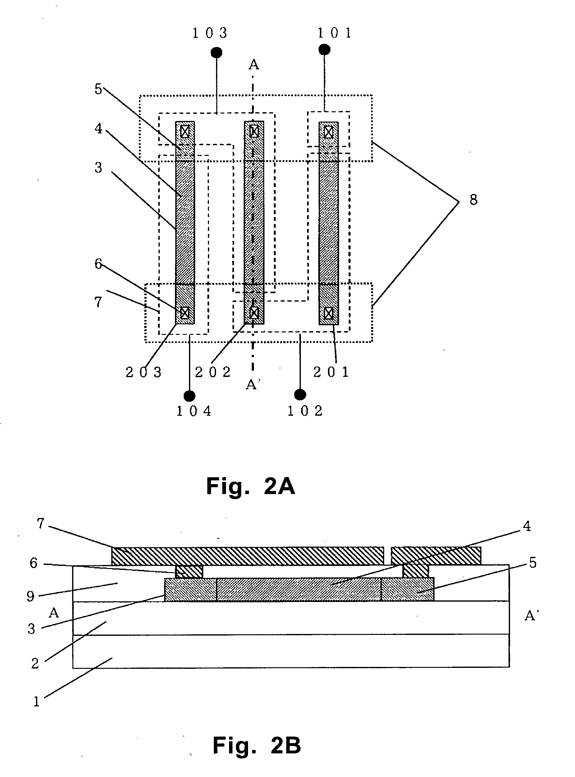
[0025]FIG. 1 shows an embodiment of the present invention for realizing a resistor circuit shown in FIG. 3. Resistors 1 (201) to 3 (203) are each formed of the polycrystalline silicon film 3 which is formed on the insulating film 2 on the semiconductor substrate 1 and which is composed of the low concentration impurity region 4 and the high concentration impurity regions 5 as in the prior art. The potential of the terminal A (101) and the terminal D (104) is taken out respectively through the metal wiring 7 via the contact holes 6 provided on the high concentration impurity regions 5.
[0026] However, in the prior art, as regards the metal wiring covering the resistor, there has been adopted the structure in which the metal wiring of one of the terminals covers the resistor connected therewith. However, in the present invention, one metal wiring covers all the resist...
PUM
 Abstract
Description
Claims
Application Information


