Tape wiring substrate and semiconductor chip package

a technology of tape wiring and semiconductor chips, applied in the direction of sustainable manufacturing/processing, semiconductor/solid-state device details, instruments, etc., can solve the problems of difficult to design the tape wiring substrate, difficulty in addressing the bonding strength, and the number of electrode pads, etc., to achieve the effect of small area and small area

Active Publication Date: 2009-09-17
LAPIS SEMICON CO LTD
View PDF10 Cites 15 Cited by
  • Summary
  • Abstract
  • Description
  • Claims
  • Application Information

AI Technical Summary

Benefits of technology

[0037]As mentioned above, it is possible to provide a semiconductor chip package which can be implemented in a small area even when the semiconductor chip is provided with a lot of electrode pads.
[0038]According to the present invention, it is possible to provide a tape wiring substrate and a semiconductor chip package which can be implemented in a small area, even when the semiconductor chip is provided with a lot of electrode pads for output.

Problems solved by technology

However, in the tape wiring board described in JP-A No. 2005-167238, since the electrode pad for the display device is formed only along one side of the semiconductor chip, it is difficult to address problems relating to bonding strength between the semiconductor chip and the tape wiring substrate when the number of electrode pads for the display device rapidly increases.
Particularly, since the wiring on the tape wiring substrate that forms an electrical connection to the electrode pad disposed at the other side of the semiconductor chip is formed so as to enter into the chip mounting and cross a line corresponding to a side orthogonal to the other side of the semiconductor chip of the chip mounting portion, it is difficult to design the tape wiring substrate.
If the orthogonal side of the semiconductor chip is short, the amount of wiring that can enter into the chip mounting portion across the orthogonal side is limited (restricted).
In other words, if the number of the electrode pads arranged at the other side of the semiconductor chip is large, the tape wiring substrate will be insufficient.
Further, since an arrangement of the output terminals of the driving IC for the display device is dependent on the input terminals of the display device side, it is necessary to employ a designated arrangement, and this makes designing the tape wiring substrate difficult.

Method used


Image

  • Tape wiring substrate and semiconductor chip package
  • Tape wiring substrate and semiconductor chip package
  • Tape wiring substrate and semiconductor chip package

Examples


Embodiment Construction

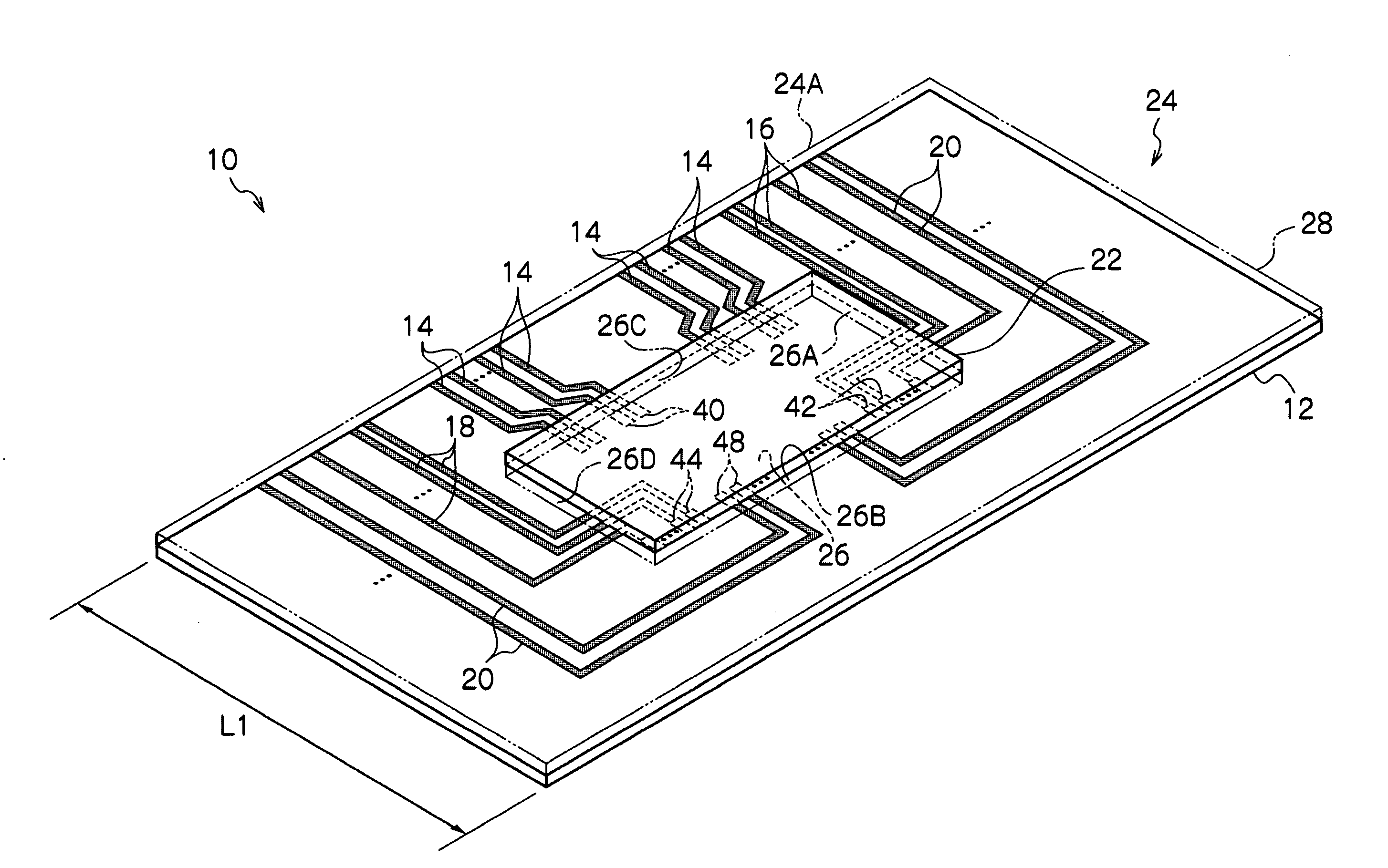
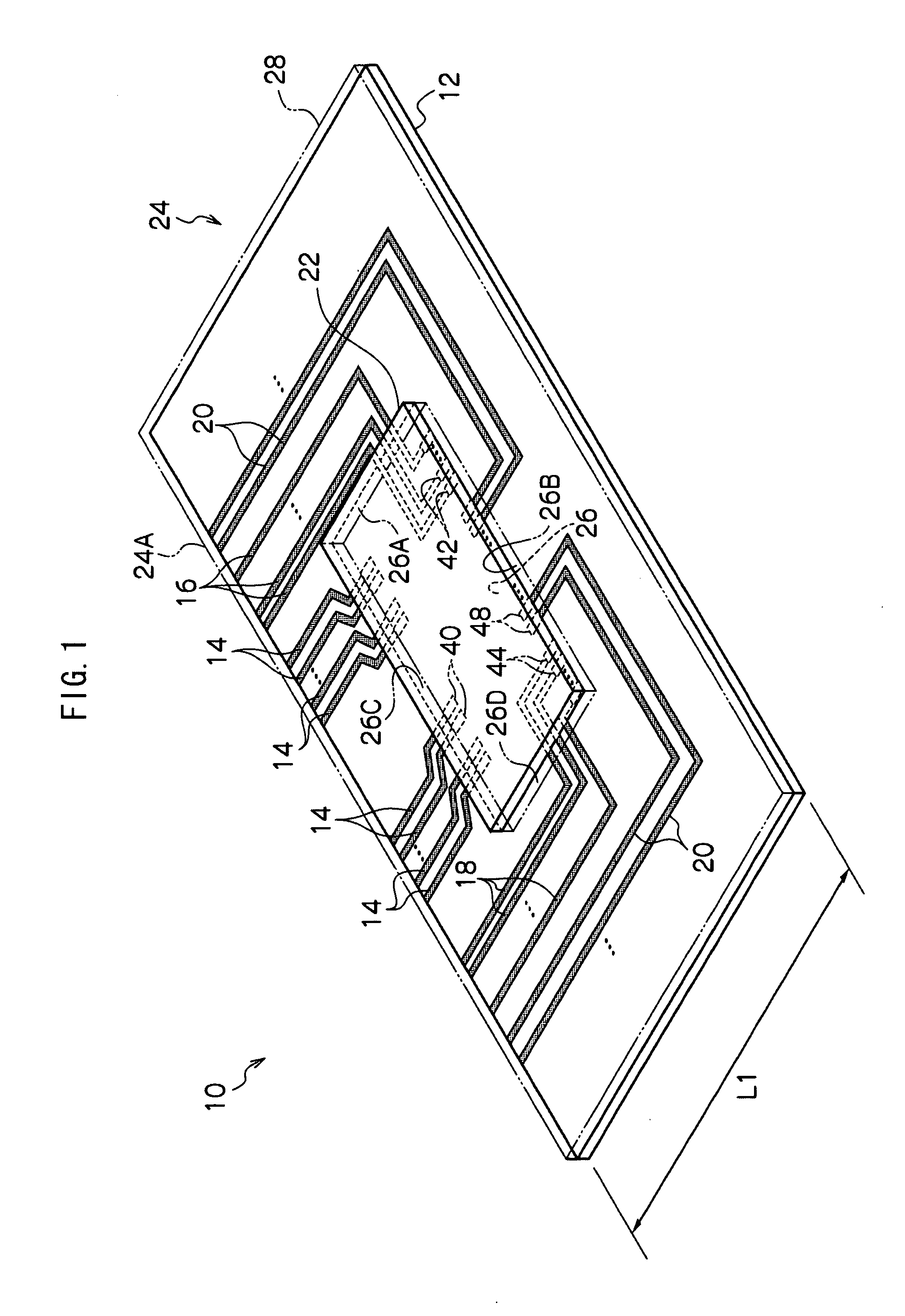
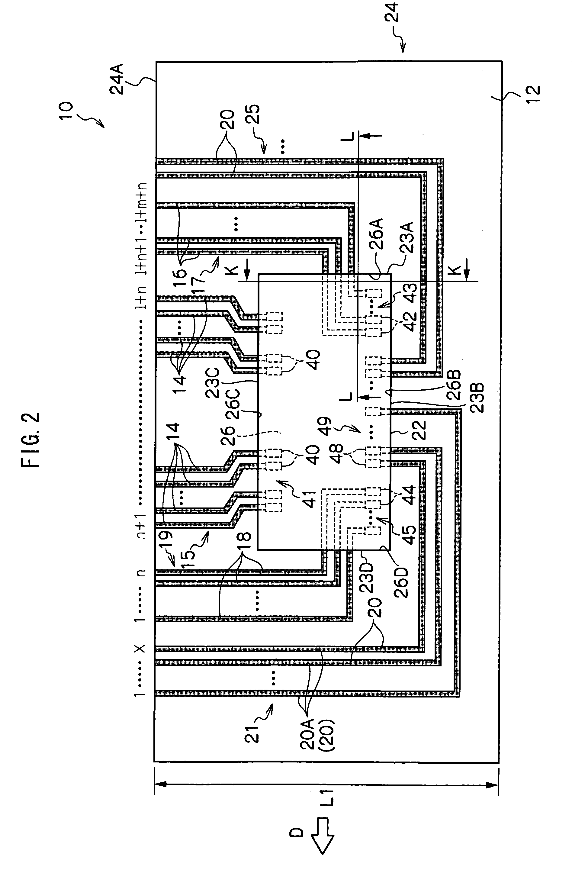
[0053]A description will be given of a tape wiring substrate in accordance with a first exemplary embodiment of the invention, and a semiconductor chip package employing the tape wiring substrate with reference to FIGS. 1 to 5.

[0054]As shown in FIGS. 1 and 2, a gate semiconductor chip package 10 as a semiconductor chip package is structured so as to include a base film 12 made of a soft material, a first output wiring 14 serving as a first wiring, a second output wiring 16 serving as a second wiring, a third output wiring 18 serving as a third wiring, an input wiring 20 serving as a fourth wiring, and a gate driving semiconductor chip 22 electrically connected to each of the wirings 16, 18 and 20.

[0055]The input wiring 20 includes a wiring to which a signal controlling the gate driving semiconductor chip 22 is input, and a wiring which outputs a signal controlling the other gate driving semiconductor chip. Accordingly, the input wiring 20 can be separately expressed by the first inp...


PUM


Abstract

A second output wiring and a third output wiring enter into a chip mounting portion while coming across a second side and a third side of the chip mounting portion. The other end portions of the second output wiring and the third output wiring enter into the chip mounting portion are bent toward a fourth side of the chip mounting portion, and are connected to an output pad and an output pad provided along a fourth side of the semiconductor chip. An input wiring extends along the fourth side of the chip mounting portion, is bent from a midstream to enter into the chip mounting portion while coming across the fourth side of the chip mounting portion, and is connected to an input pad provided along the fourth side of the semiconductor chip.

Description

CROSS-REFERENCE TO RELATED APPLICATION[0001]This application claims priority under 35 USC 119 from Japanese Patent Application No. 2008-066040, the disclosure of which is incorporated by reference herein.BACKGROUND OF THE INVENTION[0002]1. Field of the Invention[0003]The present invention relates to a tape wiring substrate and a semiconductor chip package using the same.[0004]2. Description of Related Art[0005]Together with reductions in the sales prices of display devices, a reduction in the cost of the various components thereof has been desired. This situation is also common to a driving IC (a semiconductor chip package) for display devices, and a low cost is desired even when a single tape wiring substrate is used in the driving IC. As an example thereof, a semiconductor chip package fabricated by mounting a rectangular semiconductor chip to a tape wiring substrate, in which a wiring is formed, is described in Japanese Patent Application Laid-Open (JP-A) No. 2005-167238.[0006]Th...

Claims


Application Information

Patent Timeline
Patent Type & Authority Applications(United States)
IPC IPC(8): H05K1/11H05K1/18
CPCH05K1/111H05K1/189H05K2201/09227H01L2224/16H05K2201/10674H05K2201/10681H05K2201/09781Y02P70/50
Inventor KUNIMATSU, DAISUKETAKAYANAGI, TAKEHIRO
Owner LAPIS SEMICON CO LTD
Why Eureka
Try Eureka