Reinforced probes for testing semiconductor devices

Inactive Publication Date: 2006-02-09
SV PROBE PTE LTD
View PDF28 Cites 24 Cited by
  • Summary
  • Abstract
  • Description
  • Claims
  • Application Information

AI Technical Summary

Benefits of technology

[0007] According to an exemplary embodiment, the present invention relates to a probe assembly for testing integrated circuits. The probe assembly includes a plurality of elongated probes each secured at one end of the probe to a substrate, for example, by bonding the probe to the substrate [e.g., (1) wire bonding a probe to a substrate, (2) pick and place bonding of a probe to a substrate (e.g., using an adhesive, solder, etc.), (3) plating a probe on the substrate through masking te

Problems solved by technology

Loads applied to the probes create stresses in the bonded connection between t

Method used


Image

  • Reinforced probes for testing semiconductor devices
  • Reinforced probes for testing semiconductor devices
  • Reinforced probes for testing semiconductor devices

Examples


Example

DETAILED DESCRIPTION OF THE DRAWINGS

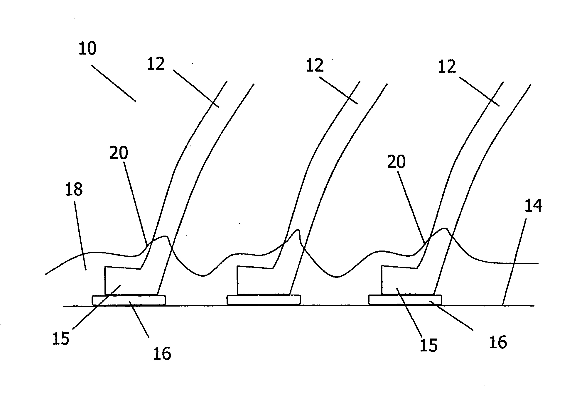
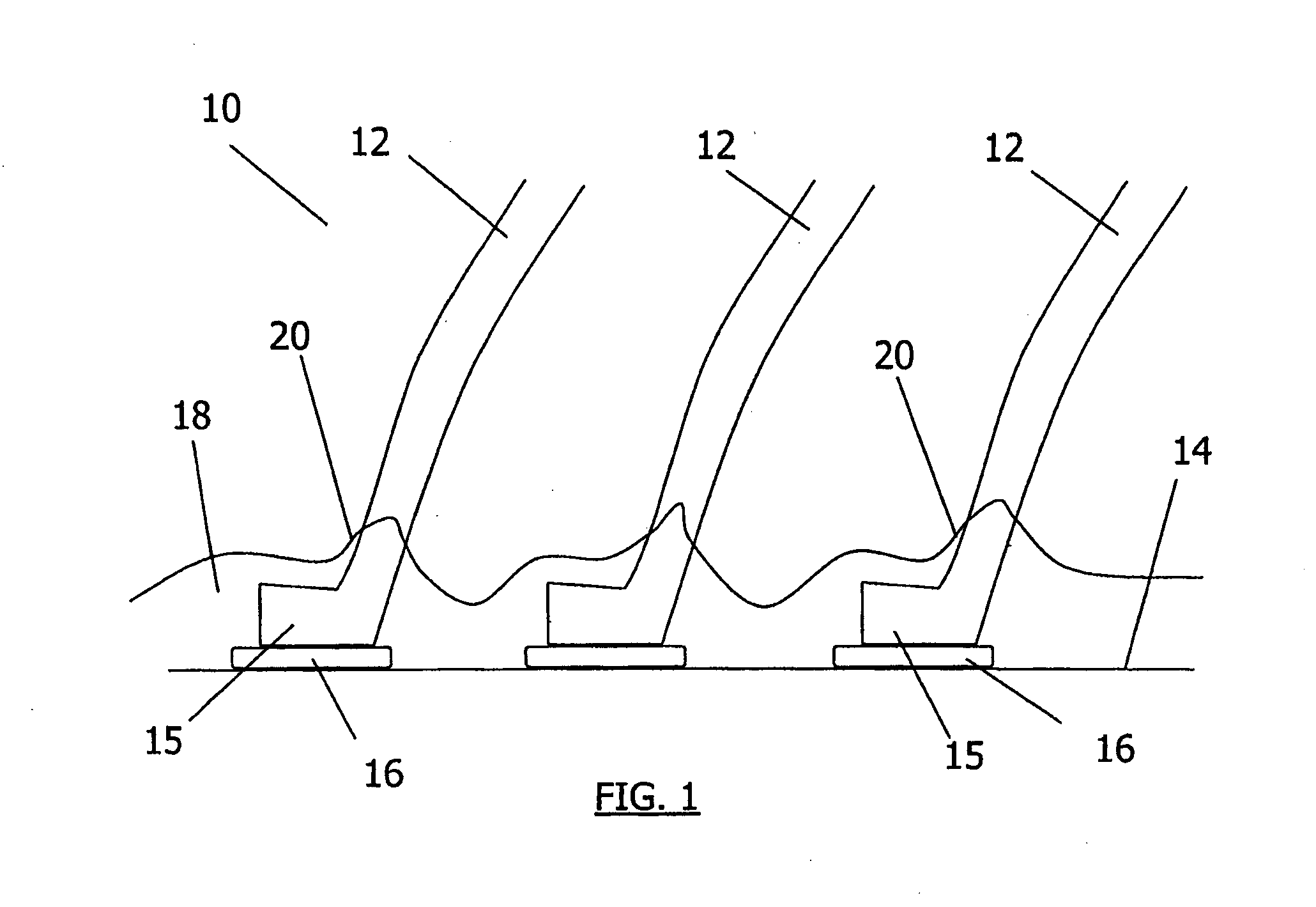
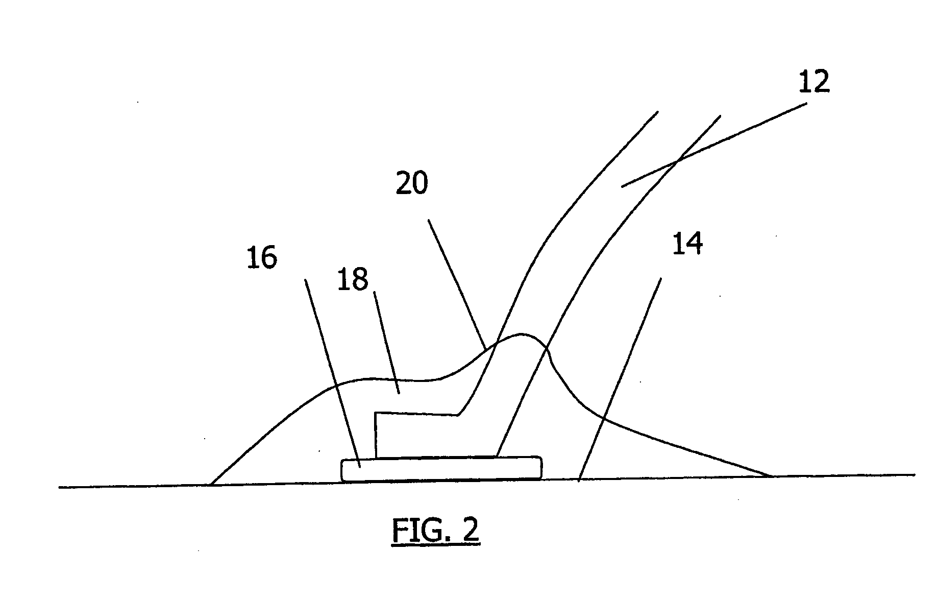
[0019] Referring to FIGS. 1 through 3, there is shown a portion of a test probe assembly 10 (e.g., a portion of a probe card assembly) according to the present invention including a plurality of elongated probes 12. The probes 12, which are shown enlarged in the figures to facilitate discussion, may be made from an electroplated material having a thickness of only a few mils. For example, the dimensions of the probes 12 may be approximately 1.0 to 4.0 mils across and approximately 3 mils thick. An exemplary probe size is approximately 2.5 mils by 3.0 mils. The present invention, in the manner described below, provides a reinforced connection between the elongated probes 12 and a substrate 14 (e.g., a space transformer).

[0020] The probe assembly 10 of the present invention will preferably form part of a probe card device that is used to test integrated circuits formed on a silicon wafer. When incorporated into a probe card device, the terminal en...


PUM


Abstract

A probe card assembly is provided. The probe card assembly includes a substrate and a plurality of probes bonded to a surface of the substrate. The probe card assembly also includes a reinforcing layer provided on the surface of the substrate. The reinforcing layer is in contact with a lower portion of each of the probes, where a remaining portion of each of the probes is free from the reinforcing layer.

Description

RELATED APPLICATIONS [0001] The present application is related to and claims priority from U.S. Provisional Application No. 60 / 589,618, filed Jul. 21, 2004, which is incorporated herein by reference in its entirety.FIELD OF THE INVENTION [0002] The present invention relates to integrity testing of semiconductor devices, and more particularly, to a test probe assembly for testing circuits formed on silicon wafers prior to dicing the wafer into chips. BACKGROUND OF THE INVENTION [0003] Integrated circuits typically include a thin chip of silicon, which is formed by dicing a wafer of silicon. Each integrated circuit includes a plurality of input / output pads that are formed on the silicon wafer. In order to assess the operational integrity of the wafer prior to dicing, the silicon wafer is subjected to testing to identify defective circuits. [0004] Known apparatuses for testing silicon wafers include a test controller, which generates integrity test signals, and a probe card, which form...

Claims


Application Information

Patent Timeline
IPC IPC(8): G01R31/02
CPCB82Y30/00G01R1/0466G01R3/00G01R1/07357G01R1/07307G01R1/067G01R31/26H01L22/00
Inventor MALANTONIO, EDWARD L.LAURENT, EDWARDHANOON, ILANHMIEL, ANDREWTUNABOYLU, BAHADIRNGUYEN, ANH-TAI THAITRAN, LICH
Owner SV PROBE PTE LTD
Why Eureka
Try Eureka