

Optical waveguide structure
a waveguide and optical technology, applied in the direction of optical waveguide light guide, instruments, optics, etc., can solve the problems of weak losses at the optical interface, waveguide technologies do not adequately address competing goals, and reduce coupling efficiency, so as to improve the packing density, and reduce the loss
- Summary
- Abstract
- Description
- Claims
- Application Information
AI Technical Summary
Benefits of technology
Problems solved by technology
Method used
Image

Examples
first embodiment
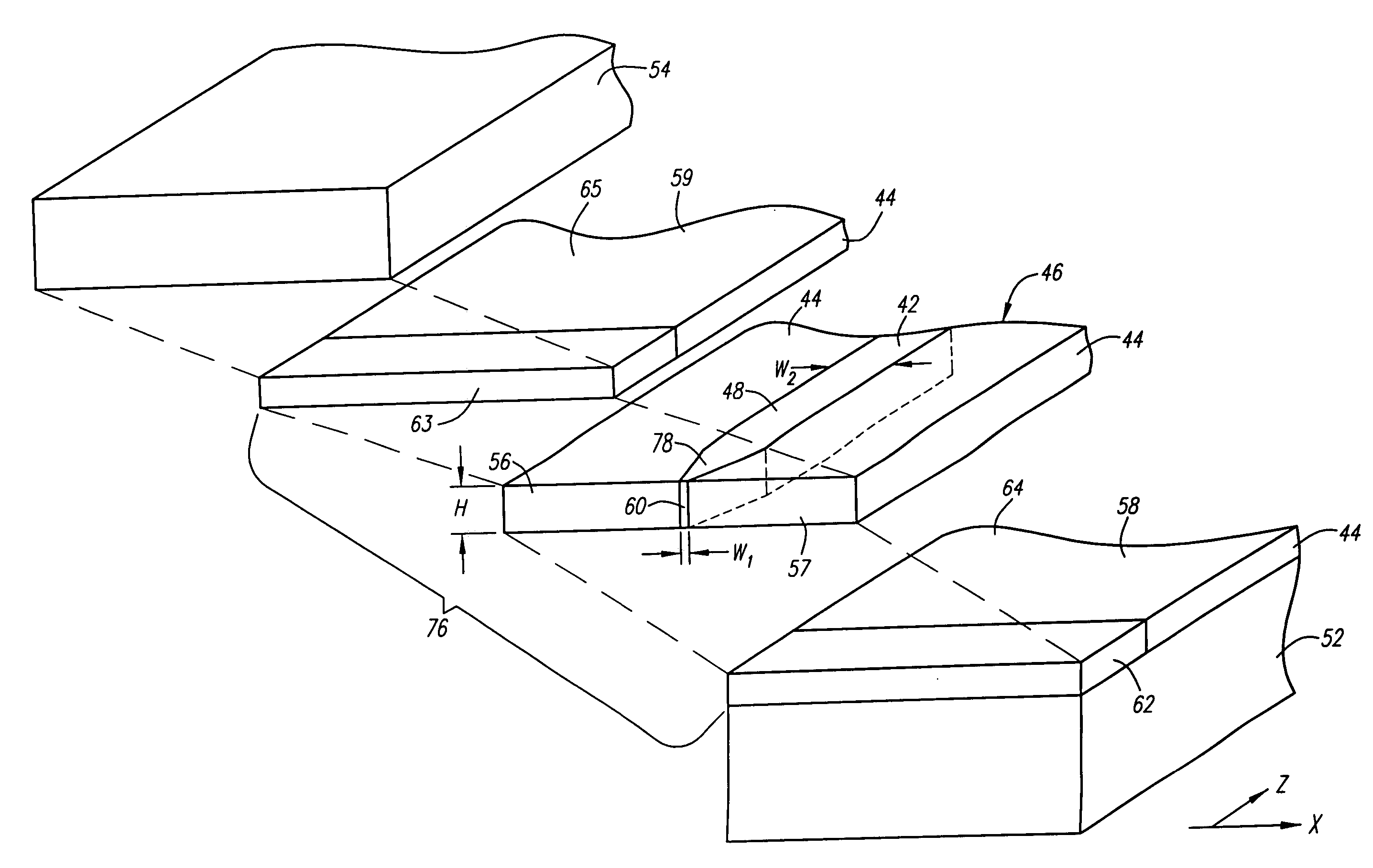
[0065]FIGS. 5-7 illustrate a waveguide structure 40 according to the invention. Waveguide structure 40 comprises core 42 and cladding material 44, which surrounds core 42. Although cladding material 44 is shown as completely surrounding core 42 in the illustrated embodiment, cladding material 44 may only partially surround core 42 in other embodiments. For example, in certain implementations, cladding material 44 may only be provided on the two lateral sides and bottom of core 42.
[0066] The waveguide structure 40 will typically be formed on a substrate 52 and form part of an integrated optical chip 38. A wide variety of substrates can be used for substrate 52, including those conventionally used in fabricating integrated optics, such as silica, silicon, indium gallium arsenide, and indium phosphide substrates. The optical chip 38 may also include a protective layer 54 formed over the waveguide structure 40. The protective layer 54 acts as a moisture barrier layer and helps protect t...
second embodiment
[0088] a waveguide structure according to the present invention is shown in FIG. 8. The principal difference between the waveguide structure 67 shown in FIG. 8 and the waveguide structure 40 of the previous embodiment resides in the refractive index profiles of the core 42 and the cladding material 44. As with the previous embodiment, the core 42 is adapted to propagate light in an axial direction along a path defined by the core. The core 42 includes a channel waveguide 48 coupled to a taper 50 that, in the present embodiment, laterally extends out from the waveguide 48. As a result, the lateral dimension, W, of the core 42 varies over the axial extent of taper 50 from W1 at its widest point to W2 at its narrowest point, which corresponds to the width of channel waveguide 48. On the other hand, the vertical dimension, H, of the core 42 preferably remains constant over the axial extent of core 42, at least within the limitations of the fabrication equipment employed.
[0089] The waveg...
third embodiment
[0106] a waveguide structure according to the present invention is shown in FIG. 10. The principal difference between the waveguide structure 76 shown in FIG. 10 and the waveguide structures 40, 67 described in connection with the previous embodiments resides in the refractive index profiles of the core 42 and the cladding material 44 and the use of a taper 78 that tapers laterally inward from channel waveguide 48 rather than tapers laterally outward from the waveguide 48.
[0107] As with the previous embodiments, the core 42 is adapted to propagate light in an axial direction along a path defined by the core. The core 42 includes a channel waveguide 48 coupled to a taper 78 that, in the present embodiment, laterally extends inward from the waveguide 48. As a result, the lateral dimension, W, of the core 42 varies over the axial extent of taper 78 from W1 at its narrowest point to W2 at its widest point, which corresponds to the width of channel waveguide 48. On the other hand, the ve...
PUM
 Abstract
Description
Claims
Application Information