

Compliant substrate for a heteroepitaxial structure and method for making same
- Summary
- Abstract
- Description
- Claims
- Application Information
AI Technical Summary
Benefits of technology
Problems solved by technology
Method used
Image

Examples
first embodiment
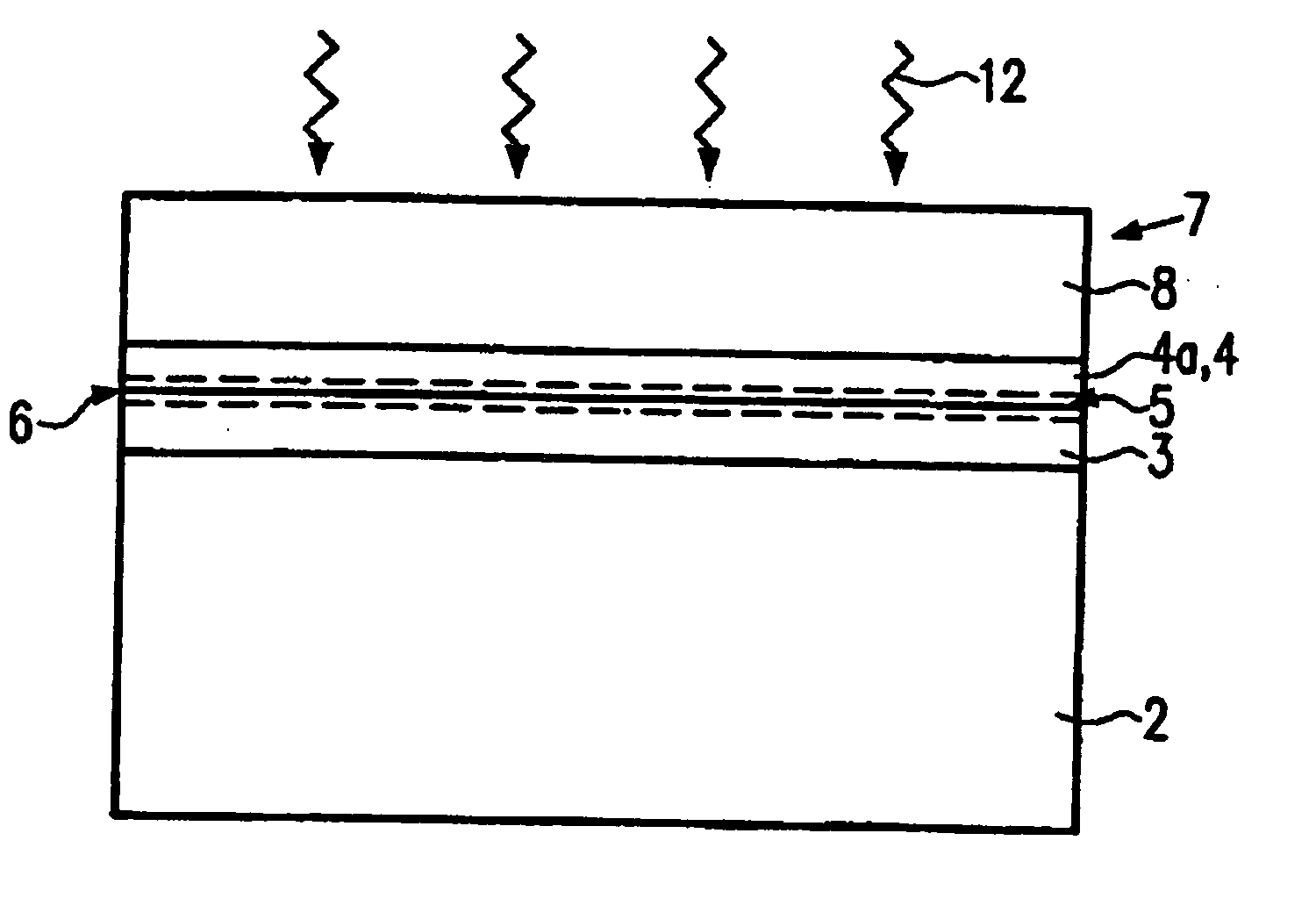
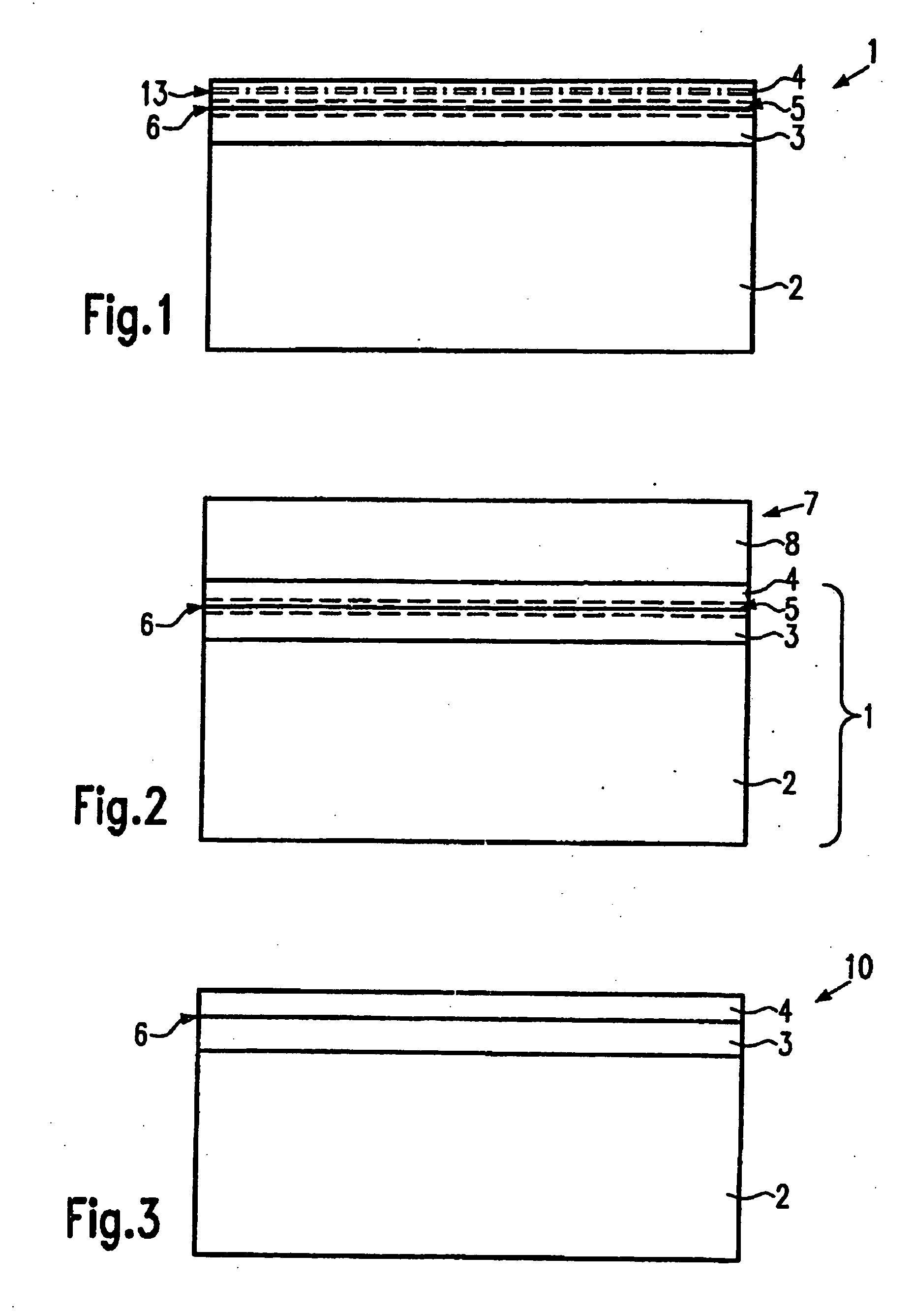
[0050] FIGS. 3 to 5 show schematically an exemplary process flow of an inventive method according to the inventive method. In accordance with a first step shown in FIG. 3, a silicon-on-insulator structure 10 or SOI-structure is fabricated. The silicon-on-insulator structure 10 can be fabricated for example by SIMOX or by Smart-cut® technology, resulting in a structure consisting of a carrier substrate 2, for instance of silicon, which is covered by a buried layer 3 of silicon dioxide and having on top a single-crystalline top layer 4 of silicon. As shown in FIG. 1, the top layer 4 and the buried layer 3 form an interface 6 therebetween.
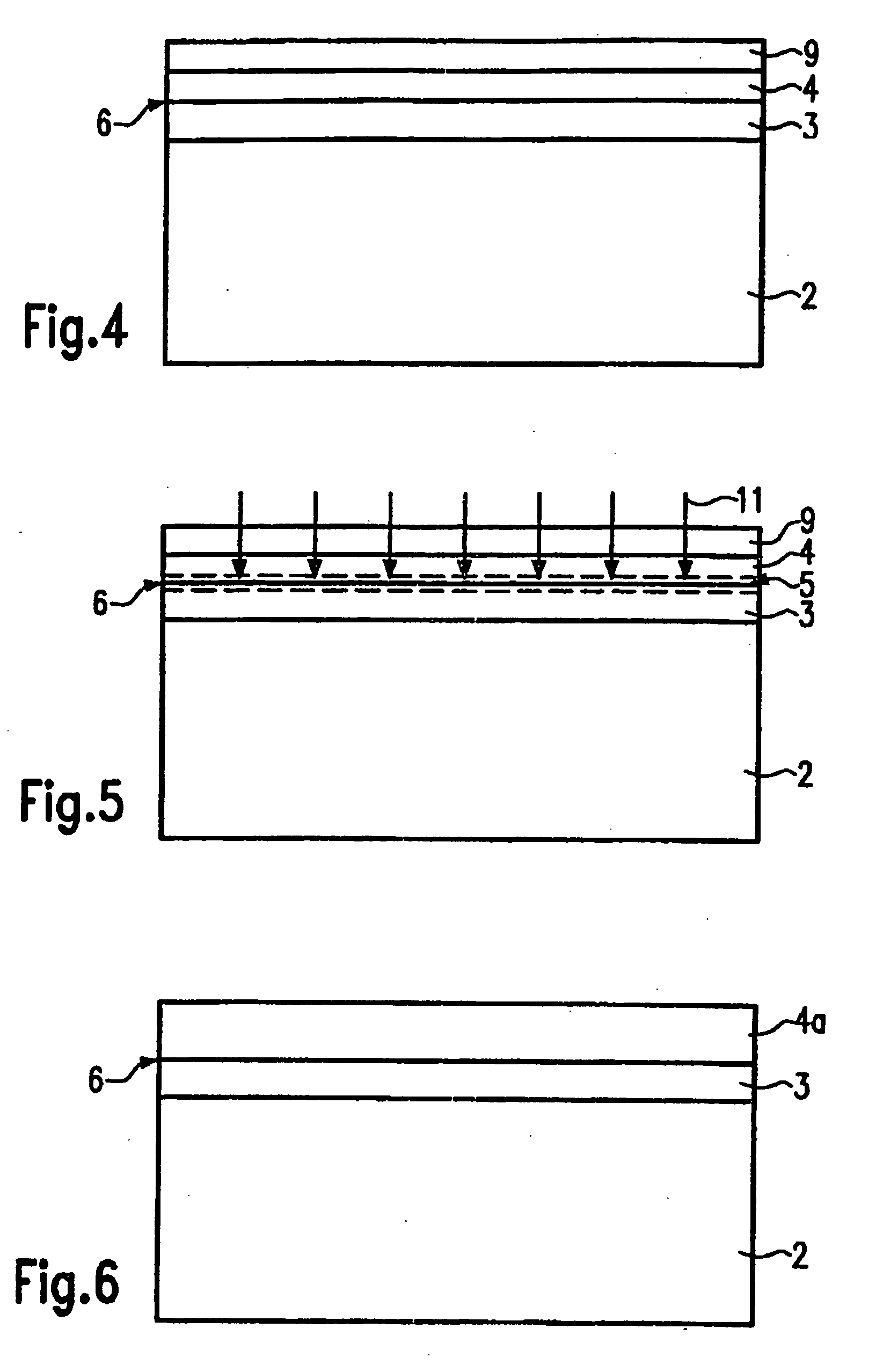
[0051]FIG. 4 shows the silicon-on-insulator structure of FIG. 3 after a further step in which an auxiliary layer 9 such as a silicon dioxide layer is deposited on the top layer 4. Any other material known in the art which can easily be deposited and then removed from the top layer 4 can be used Instead of silicon dioxide as auxiliary layer 9.
[0052]FI...
second embodiment
[0056] FIGS. 6 to 8 show schematically an exemplary process flow of the inventive method.
[0057]FIG. 6 shows schematically a side view of a silicon-on-insulator structure 10a, which has been fabricated in a first step. The silicon-on-insulator structure may be fabricated, for instance, by SIMOX or by Smart-cut® technology, resulting in a structure consisting of carrier substrate 2 such as a silicon substrate covered by a buried layer 3 of silicon dioxide having on top a thick single-crystalline top layer 4a of silicon with a thickness of about 500 nm. Preferably, the thick single-crystalline top layer 4 has a thickness of about several hundred nanometers. Between the top layer 4a and the buried layer 3 an interface 6 is formed.
[0058]FIG. 7 shows the silicon-on-insulator structure 10a of FIG. 6 during an implantation step in which species 11 are implanted through the thick top layer 4a into a relatively thin region 5 at or near the interface 6 between the thick top layer 4a and the b...
PUM
 Abstract
Description
Claims
Application Information