Correction of non-uniform sensitivity in an image array

a technology of image array and sensitivity, applied in the field of complementary metal oxide semiconductor (cmos) imager, can solve the problems of sensitivity variation over the array, unsatisfactory parts, adversely affecting the image produced by the aps,

Active Publication Date: 2006-02-16
MICRON TECH INC
View PDF17 Cites 209 Cited by
  • Summary
  • Abstract
  • Description
  • Claims
  • Application Information

AI Technical Summary

Problems solved by technology

The different parts are not ideal, of course, and can produce sensitivity variations over the array.
Most of the components described above, due to imperfections or practical limitations, may contribute to spatial signal attenuation, which in turn results in a sensitivity variation over the array.
This phenomenon can adversely effect the images produced by the APS.
Since pixel sensitivity depends in part on the geometric location of a given pixel, generally speaking, one “global” correction function is not satisfactory.
The boundaries of the zones, however, cannot be modified to accommodate any other lenses that may be used.
One disadvantage of the prior art is that the zones of known correction algorithms are fixed by design.
That is, while a given non-uniform sensitivity correction algorithm may work well for a given type of lens, the algorithm does not work as well with another type of lens.
Another disadvantage associated with the prior art is that when the center of the lens is not perfectly aligned with the center of the APS array, as is often the case, there is currently no method to take that offset into account and to adjust the zone boundaries for it.

Method used


Image

  • Correction of non-uniform sensitivity in an image array
  • Correction of non-uniform sensitivity in an image array
  • Correction of non-uniform sensitivity in an image array

Examples


Embodiment Construction

[0021] In the following detailed description, reference is made to the accompanying drawings which form a part hereof, and in which is shown by way of illustration specific embodiments in which the invention may be practiced. These embodiments are described in sufficient detail to enable those of ordinary skill in the art to make and use the invention, and it is to be understood that structural, logical or procedural changes may be made to the specific embodiments disclosed without departing from the spirit and scope of the present invention.

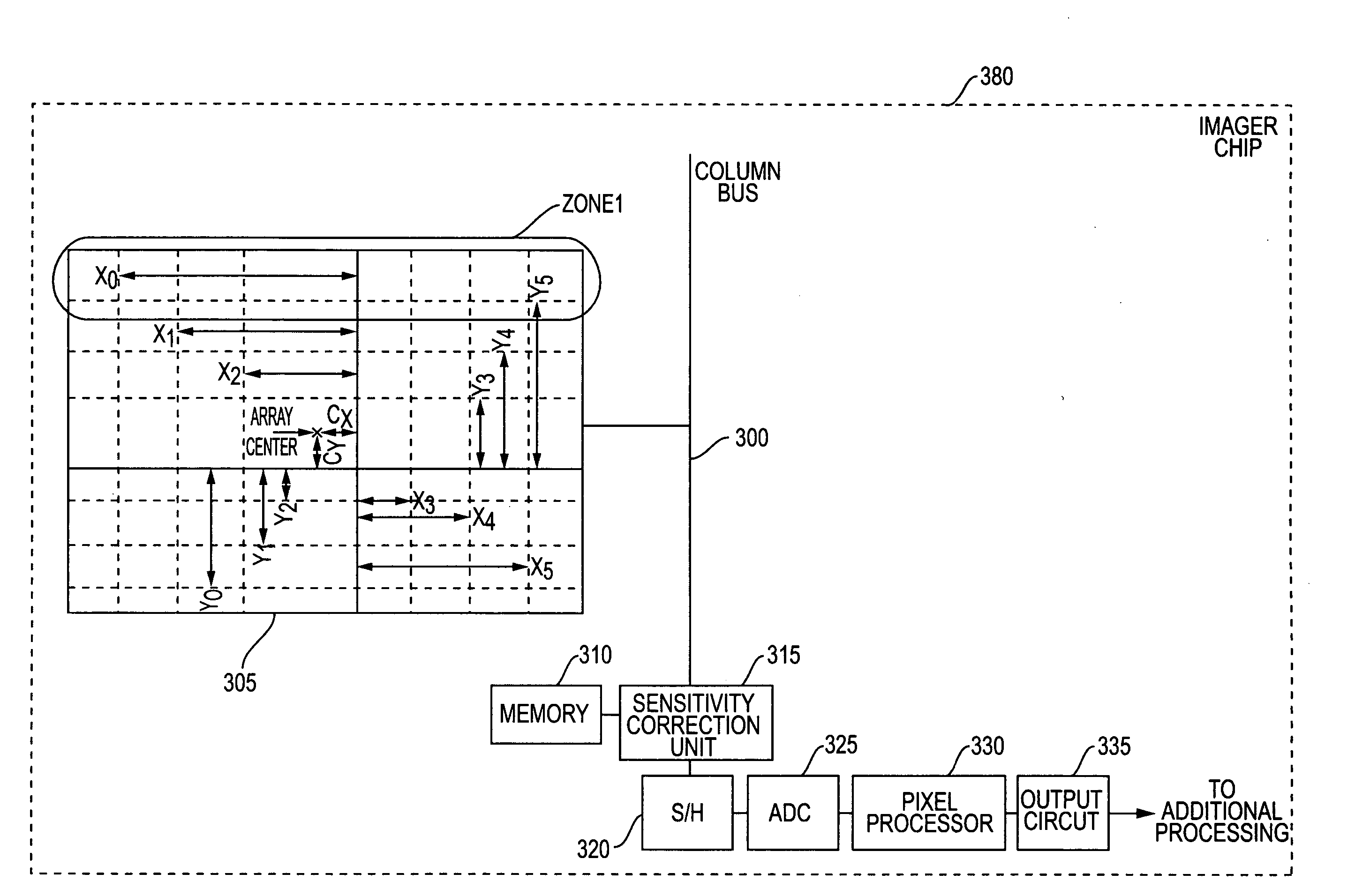
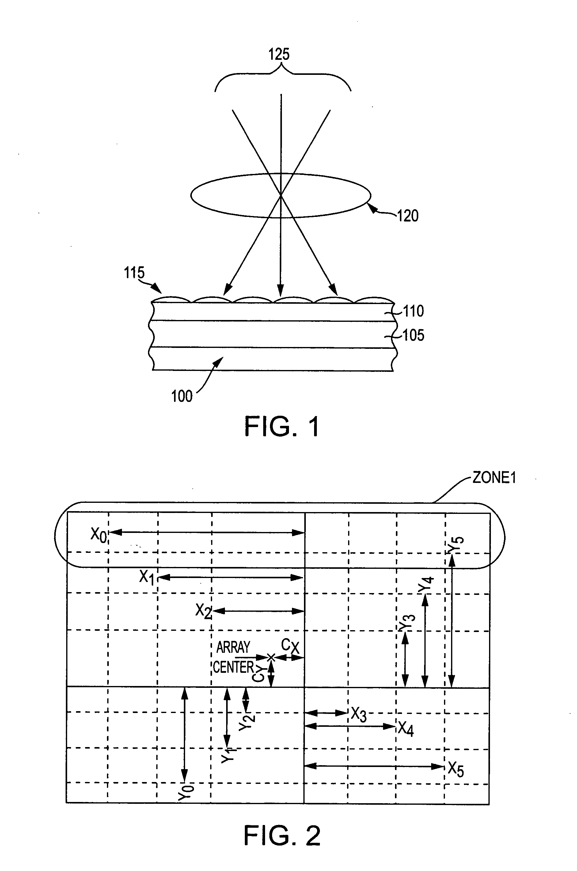
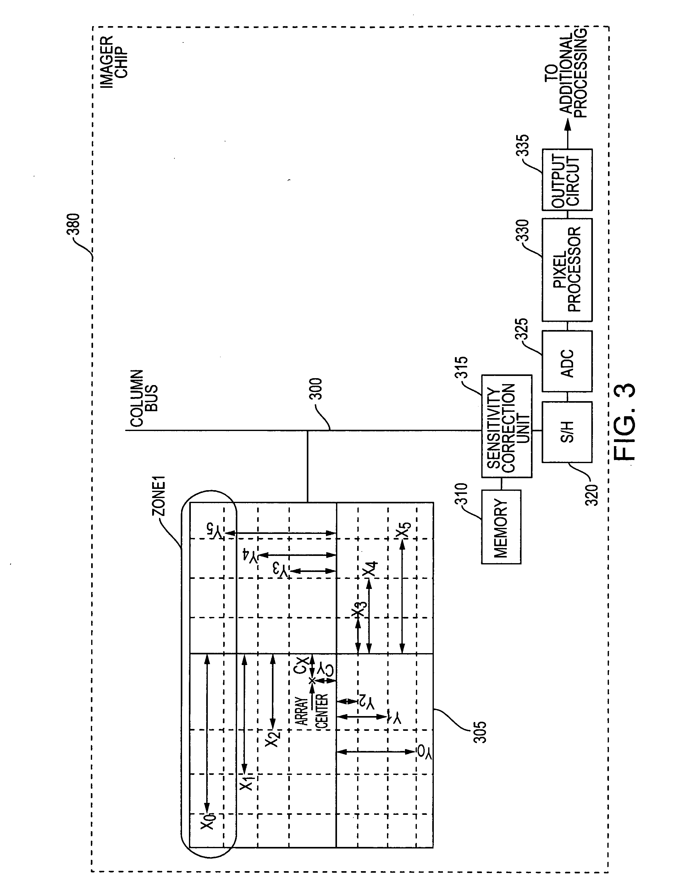
[0022]FIG. 2 depicts an APS array divided into several zones, in accordance with an exemplary embodiment of the invention. The zones depicted in FIG. 2 represent the optimum geographic location of the zones when the APS array is used in conjunction with a certain type of lens. The boundaries of the zones are programmable and may be modified to another configuration so that the APS array may be used with another type of lens. As depicted, the ar...


PUM


Abstract

An improved non-uniform sensitivity correction algorithm for use in an imager device (e.g., a CMOS APS). The algorithm provides zones having flexible boundaries which can be reconfigured depending upon the type of lens being used in a given application. Each pixel within each zone is multiplied by a correction factor dependent upon the particular zone while the pixel is being read out from the array. The amount of sensitivity adjustment required for a given pixel depends on the type of lens being used, and the same correction unit can be used with multiple lenses where the zone boundaries and the correction factors are adjusted for each lens. In addition, the algorithm makes adjustments to the zone boundaries based upon a misalignment between the centers of the lens being used and the APS array.

Description

FIELD OF THE INVENTION [0001] The present invention relates generally to complementary metal oxide semiconductor (CMOS) imagers, and more particularly to correction of non-uniform sensitivity in pixels of such imagers. BACKGROUND OF THE INVENTION [0002] A CMOS image sensor is an imaging device built with CMOS technology for capturing and processing light signals. Results produced by the CMOS image sensor can be displayed. A type of CMOS image sensors, called a CMOS Active Pixel Sensors (APS), has been shown to be particularly suited for handheld imaging applications. [0003] The CMOS APS comprises an array of pixel processing elements, each of which processes a corresponding pixel of a received image. Each of the pixel processing elements includes a photo-detector element (e.g., a photodiode or a photogate) for detecting brightness information in the received image, and active transistors (e.g., an amplifier) for reading out and amplifying the light signals in the received image. The...

Claims


Application Information

Patent Timeline
Patent Type & Authority Applications(United States)
IPC IPC(8): H01L27/00
CPCH04N5/3572H04N25/61
Inventor JERDEV, DMITRISUBBOTIN, IGOROVSIANNIKOV, ILIA
Owner MICRON TECH INC
Why Eureka
Try Eureka