Light emitting diode lamp and light emitting diode display unit

a technology of light-emitting diodes and display units, which is applied in the direction of lighting and heating equipment, instruments, and ways, can solve the problems of remarkable deterioration of the display quality less recognition of the led display board, and degradation of display quality, so as to prevent misrecognition

Inactive Publication Date: 2006-02-23
SHARP KK
View PDF0 Cites 84 Cited by
  • Summary
  • Abstract
  • Description
  • Claims
  • Application Information

AI Technical Summary

Benefits of technology

[0009] Accordingly, it is an object of the present invention to provide an LED lamp and an LED display unit capable of preventing

Problems solved by technology

This phenomenon lessens a contrast ratio of a lit LED lamp to an unlit LED lamp, which may make the LED display board less recognizable.
This phenomenon, which is similar to misread of signalers due to afternoon sunlight, causes remarkable deterioration of display quality of the LED display board that constitutes electronic billboards, signboards, and the like.
Consequently, the apparent luminescence intensity becomes remarkably different between a view from the front side and a view with a viewpoint slightly displaced downward from the front side, thereby causing degradation of display quality.
Also, when the positional relationship between the light emitting diode chip and the interface of the lenses is changed due to production variations, the emission angle at the above-m

Method used


Image

  • Light emitting diode lamp and light emitting diode display unit
  • Light emitting diode lamp and light emitting diode display unit
  • Light emitting diode lamp and light emitting diode display unit

Examples


first embodiment

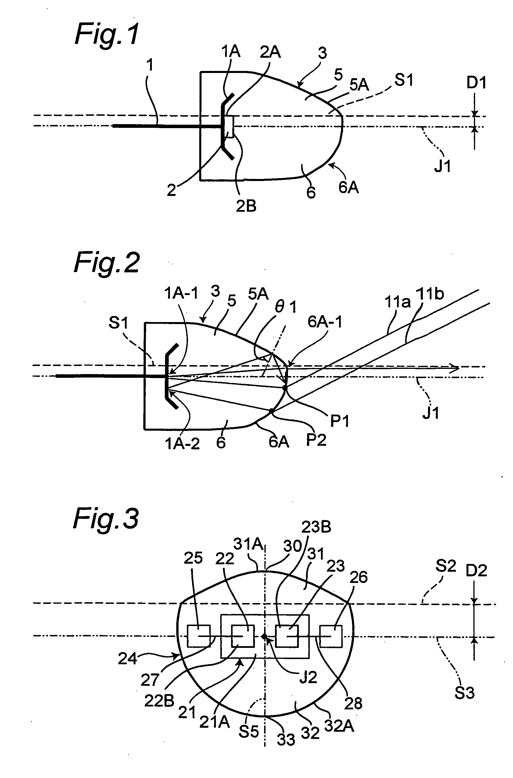
[0054]FIG. 1 shows an LED lamp in a first embodiment of the present invention seen from the side. In the first embodiment, an LED chip 2 is mounted on a cup-shaped mounting portion 1A of a lead frame 1. The LED chip 2 and the mounting portion 1A are embedded in a convex lens 3 made of resin. The resin convex lens 3 forms a convex lens protruding in the emission direction of rays of light from the LED chip 2, and has an upper portion 5 including an upper curved surface 5A exemplifying a curved surface on one side and a lower portion 6 including a lower curved surface 6A exemplifying a curved surface on the other side. In operation, the LED lamp uses a direction perpendicular to a light emitting surface 2B of the LED chip 2 as a frontward direction and the direction parallel to the light emitting surface 2B as an upward / downward direction. In use, the upper portion 5 is located on the upper side while the lower portion 6 is located on the lower side.

[0055] An interface plane S1 betwe...

second embodiment

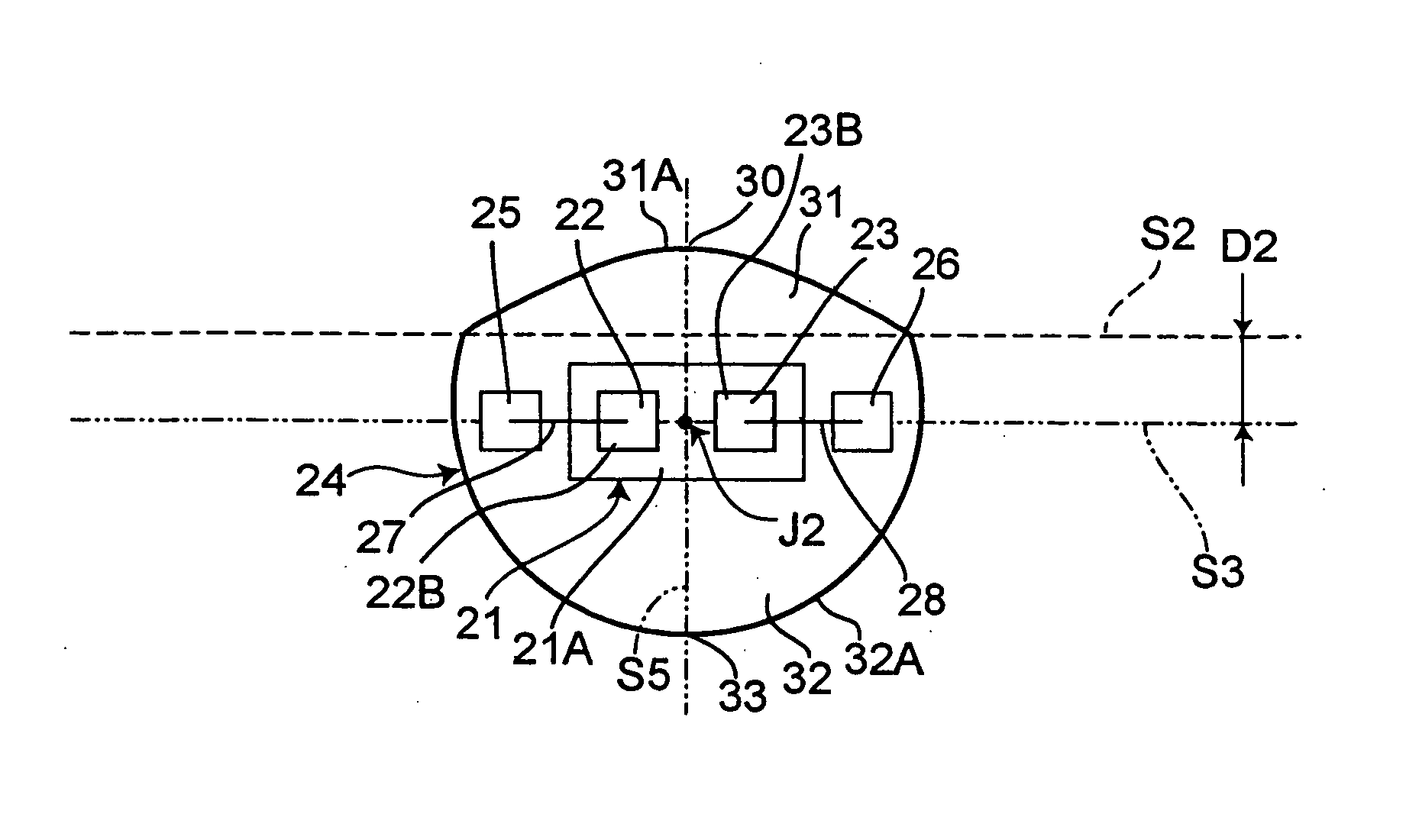
[0062] Next, FIG. 3 shows an LED lamp in a second embodiment of the present invention seen from the front side. In the second embodiment, two LED chips 22, 23 are mounted on a mounting portion 21A of a lead frame 21. These two LED chips 22, 23 are connected to respective electrode leads 25, 26 on both sides of the lead frame 21 through connection wires 27, 28.

[0063] The mounting portion 21A, the two LED chips 22, 23, and the electrode leads 25, 26 are embedded in a convex lens 24 made of resin. The convex lens 24 is convex toward the light emitting direction of the two LED chips 22, 23. The convex lens 24 is composed of an upper portion 31 and a lower portion 32 which abut on each other in an interface plane S2. The interface plane S2 is a plane that is orthogonal to an extension of light emitting surfaces 22B, 23B of the LED chips 22, 23 and does not pass the LED chips 22, 23. In operation, the LED lamp uses the direction perpendicular to the light emitting surfaces 22B, 23B of th...

third embodiment

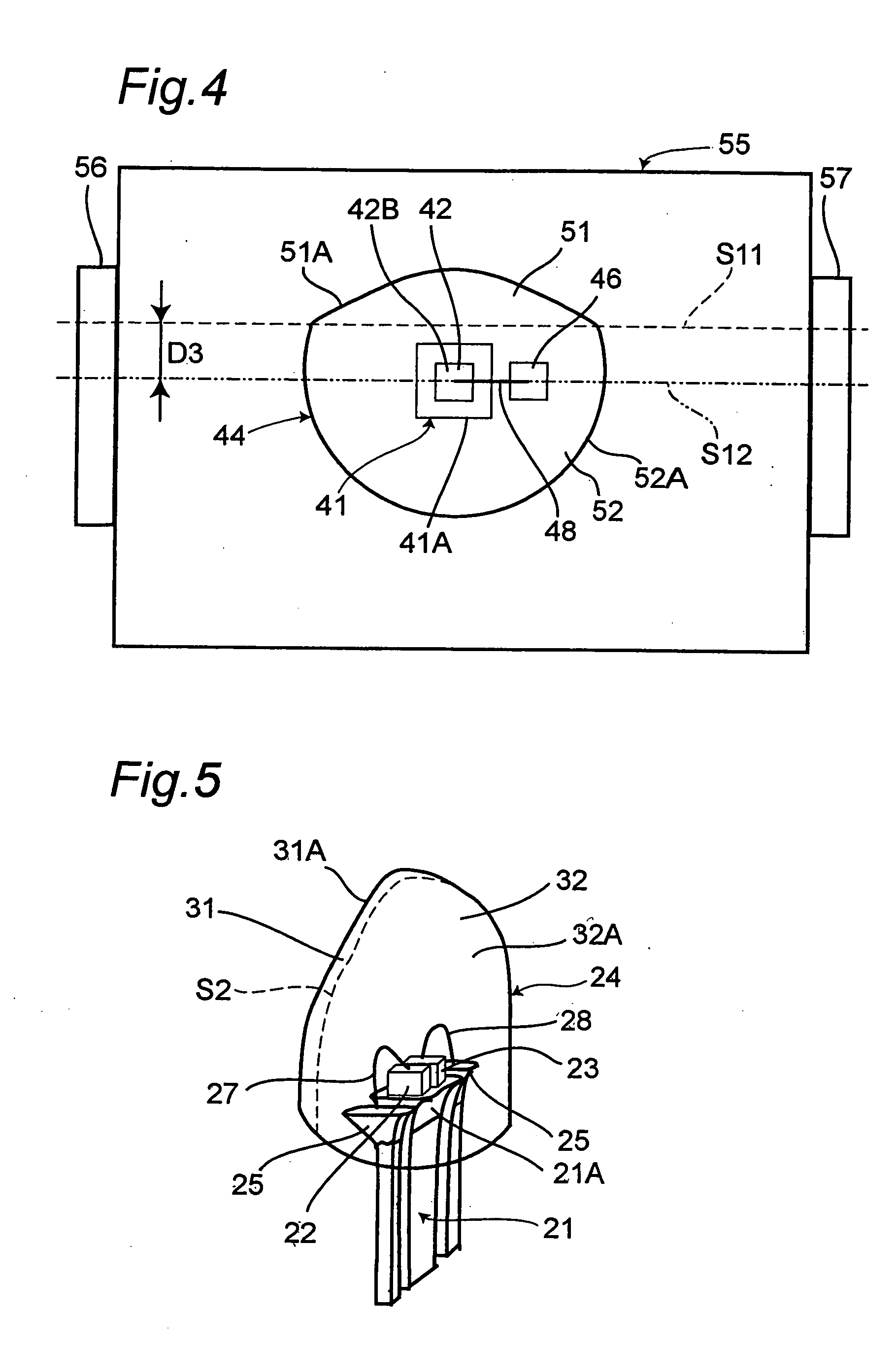
[0067] Next, FIG. 4 shows an LED lamp in a third embodiment of the present invention seen from the front side. In the third embodiment, an LED chip 42 is mounted on a mounting surface 41A of a lead frame 41, and the LED chip 42 is connected to an electrode lead 46 through a connection wire 48.

[0068] The lead frame 41, the LED chip 42, and the electrode lead 46 are embedded in a convex lens 44 made of resin. The convex lens 44 is convex toward the light emitting direction of the LED chip 42 (i.e., a direction perpendicular to the drawing sheet). The convex lens 44 is mounted on a body 55 made of resin. On both sides of the body 55, there are disposed connection terminals 56, 57 for connection to a printed wiring board (unshown). The connection terminal 56 is electrically connected to the lead frame 41 while the connection terminal 57 is electrically connected to the electrode lead 46.

[0069] The LED lamp, during operation, uses the direction perpendicular to a light emitting surface...


PUM


Abstract

An LED lamp has a convex lens 3 which has an upper portion 5 and a lower portion 6. An upper curved surface 5A of the upper portion is different in shape from a lower curved surface 6A of the lower portion 6 so as to refract rays of light from an LED chip 2 more strongly than the lower curved surface 6A does. This avoids reflection of incident outside light toward a front and hence prevents misrecognition. An interface plane S1 between the upper and lower portions 5 and 6 of the convex lens 3 is located on an upper end face 2A to thereby prevent collection of outgoing light upon the interface plane S1 and generation of an irregular emission peak at the front.

Description

BACKGROUND OF THE INVENTION [0001] The present invention relates to a light emitting diode (“LED”) lamp and an LED display unit, which are preferably used, for example, in outdoor LED display boards for displaying road information such as traffic information as well as for outdoor display for advertisement, signalers and the like. [0002] Conventionally, there has been an LED lamp shown in FIG. 10. This LED lamp is structured such that an LED chip 102 mounted on a lead frame 101 is resin-molded and embedded in a resin lens 103. The resin lens 103 has a curved surface 103A that is curved in a convex shape in the light emitting direction of the LED chip 102 (see Japanese Patent Laid-Open Publication HEI 11-154766 and Japanese Patent Laid-Open Publication HEI 10-22529, for example). [0003] The conventional LED lamp shown in FIG. 10 produces a phenomenon, when used in an outdoor LED display board for example, that in the evening and early morning when an irradiation angle of sunlight is ...

Claims


Application Information

Patent Timeline
IPC IPC(8): F21V5/00F21W111/02F21V5/04F21Y101/02G08G1/095H01L25/075H01L33/54H01L33/62
CPCH01L25/0753H01L33/54H01L2224/48091H01L2224/48247Y10S362/80H01L2924/00014H01L2924/00
Inventor KATOH, MASAAKIOMOTO, MASATOSHIMIYATA, MASATAKATAKASUGI, KEIJISEKO, MASAHIRO
Owner SHARP KK
Why Eureka
Try Eureka