Electric charged particle beam microscopy and electric charged particle beam microscope

a technology of electric charge and particle beam, which is applied in the field of electric charge particle beam microscopy and electric charge particle beam microscope, can solve the problems of geometric distortion measurement error error, inability to measure geometric distortion with high precision, and inability to make the measurement error of geometric distortion smaller than the dimensional error of the standard specimen, etc., to achieve high precision, improve length measurement precision, and high precision

Inactive Publication Date: 2009-12-15
HITACHI HIGH-TECH CORP
View PDF11 Cites 13 Cited by
  • Summary
  • Abstract
  • Description
  • Claims
  • Application Information

AI Technical Summary

Benefits of technology

[0009]According to the present invention, it is possible to measure the geometric distortion with high precision even at a magnification where the high-precision standard specimen does not exist, and correct the geometric distortion. For that reason, a length measurement precision is improved without any variation at the arbitrary magnification. Also, since the geometric distortion can be corrected with high precision, misidentification can be prevented even when the defect inspection of the specimen is conducted, to thereby improve the defect detection efficiency.

Problems solved by technology

An error in the measured geometric distortion depends on an analysis error of the image processing and a dimensional error in the known structure.
It is impossible that the geometric distortion measurement error is made smaller than the dimensional error of the standard specimen.
Accordingly, the geometric distortion cannot be measured with a high precision, and a high-precision image cannot be conducted, at the magnification where no high-precision standard specimen exists.
Also, in conducting the defect inspection of the specimen, when a difference image is calculated by an image that is insufficiently corrected, that is, an image having the geometric distortion, the geometric distortion may be misidentified as a defect.

Method used


Image

  • Electric charged particle beam microscopy and electric charged particle beam microscope
  • Electric charged particle beam microscopy and electric charged particle beam microscope
  • Electric charged particle beam microscopy and electric charged particle beam microscope

Examples


first embodiment

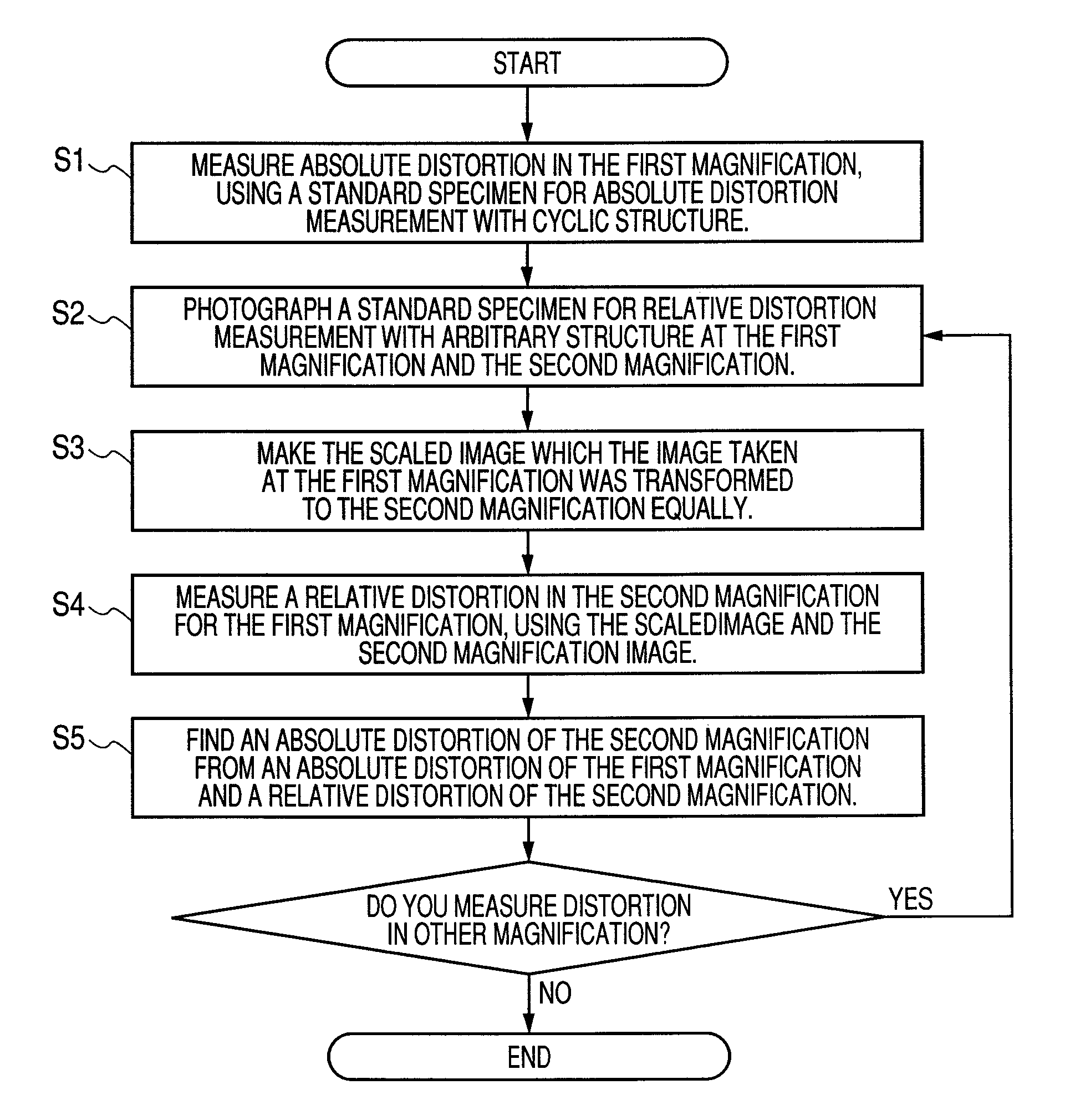
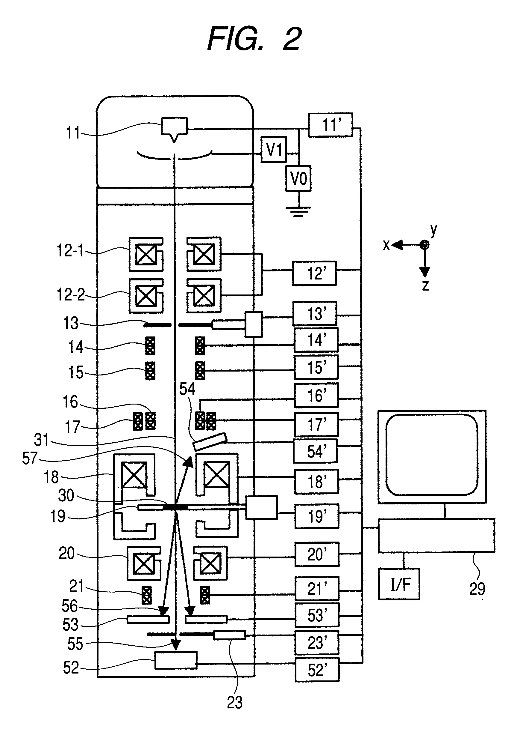
[0030]In this embodiment, a geometric distortion correcting technique is applied to a STEM / SEM. FIG. 2 shows a basic structural diagram of the STEM / SEM used in this embodiment. The STEM / SEM includes an electron gun 11 that generates a primary electron beam 31, an electron gun control unit 11′ that controls an acceleration voltage and an extraction voltage of the primary electron beam 31, a condenser lens 12 that converges the primary electron beam 31, a condenser lens control unit 12′ that controls a current value of the condenser lens 12, a condenser aperture 13 that controls the spread angle of the primary electron beam 31, a condenser aperture control unit 13′ that controls a position of the condenser aperture 13. The STEM / SEM also includes an alignment deflector 14 that controls an incident angle with respect to a specimen 30, an alignment deflector control unit 14′ that controls a current value of the alignment deflector 14, a stigmator 15 that corrects the beam configuration o...

second embodiment

[0062]This embodiment shows a geometric distortion correcting technique in the TEM. FIG. 13 shows a basic structural diagram of a TEM used in this embodiment. The TEM includes an electron gun 11 that generates a primary electron beam 31, an electron gun control unit 11′ that controls an acceleration voltage and an extraction voltage of the primary electron beam 31, a condenser lens 12 that adjusts the convergence conditions of the primary electron beam 31, a condenser lens control unit 12′ that controls a current value of the condenser lens 12, a condenser aperture 13 that controls the spread angle of the primary electron beam 31, a condenser aperture control unit 13′ that controls a position of the condenser aperture 13. The STEM / SEM also includes an alignment deflector 14 that controls an incident angle of the primary electron beam 31 that is input to a specimen 30, an alignment deflector control unit 14′ that controls a current value of the alignment deflector 14, a stigmator 15 ...

third embodiment

[0065]This embodiment shows a geometric distortion correcting technique in the wafer correspondence SEM. The basis structural diagram of the wave correspondence SEM used in this embodiment is shown in FIG. 14. The SEM includes an electron gun 11 that generates a primary electron beam 31, an electron gun control unit 11′ that controls an acceleration voltage and an extraction voltage of the primary electron beam 31, a condenser lens 12 that adjusts the convergence conditions of the primary electron beam 31, a condenser lens control unit 12′ that controls a current value of the condenser lens 12, an alignment deflector 14 that adjusts an incident angle of the primary electron beam 31 that is input to a specimen 30, an alignment deflector control unit 14′ that controls a current value of the alignment deflector 14, a stigmator 15 that adjusts the beam configuration of the primary electron beam 31 which is input to the specimen 30, and a stigmators control unit 15′ that controls a curre...


PUM


Abstract

An electric charged particle beam microscope measures a geometric distortion at an arbitrary magnification with high precision, and corrects the geometric distortion. A geometric distortion at a first magnification is measured as an absolute distortion based on a standard specimen having a cyclic structure. A microscopic structure specimen is photographed at a geometric distortion measured first magnification and at a geometric distortion unmeasured second magnification. The image at the first magnification is equally transformed to the second magnification to generate a scaled image. The geometric distortion at the second magnification is measured as a relative distortion based on the scaled image. The absolute distortion at the second magnification is obtained on the basis of the absolute distortion at the first magnification and the relative distortion at the second magnification. Subsequently, the second magnification is replaced with the first magnification, and the relative distortion measurement is repeated.

Description

CLAIM OF PRIORITY[0001]The present application claims priority from Japanese application JP 2006-187385 filed on Jul. 7, 2006, the content of which is hereby incorporated by reference into this application.FIELD OF THE INVENTION[0002]The present invention relates to an electric charged particle beam device that measures the dimensions of a specimen, and an inspection device used for a pattern inspection of a semiconductor device.BACKGROUND OF THE INVENTION[0003]As a device for visualizing the configuration of a specimen with precision of nm (nanometer), there are a SEM (scanning electron microscope), a STEM (scanning transmission electron microscope), and a TEM (transmission electron microscope). The SEM and STEM are devices that raster-scans the specimen with an electron beam that has been converged to the order of nm, detects a signal that is generated from an electron beam irradiated area, and synchronizes the signal with raster scanning to form an image. The TEM is a device that...

Claims


Application Information

Patent Timeline
Patent Type & Authority Patents(United States)
IPC IPC(8): H01J37/153
CPCG06T5/006H01J37/1475H01J37/153H01J37/222H01J37/263H01J37/28H01J2237/3045H01J2237/1536H01J2237/221H01J2237/28H01J2237/2802H01J2237/2818H01J2237/2826H01J2237/1526
Inventor TSUNETA, RURIKOKOGUCHI, MASANARIINADA, HIROMI
Owner HITACHI HIGH-TECH CORP
Why Eureka
Try Eureka