Method for filling electrically different features

a technology of electrically different features and filling methods, which is applied in the direction of semiconductor/solid-state device manufacturing, basic electric elements, electric apparatus, etc., can solve the problems of uneven activation, difficult bottom-up filling process, etc., to achieve fast, reliable and uniform plating, low surface potential area, and easy bottom-up filling process

Inactive Publication Date: 2006-03-02
MICRON TECH INC
View PDF15 Cites 22 Cited by
  • Summary
  • Abstract
  • Description
  • Claims
  • Application Information

AI Technical Summary

Benefits of technology

[0015] Advantageously, the invention provides an easy process for bottom up filling of multiple high aspect ratio features on a substrate. Fabricating contacts according to the present invention achieves a fast, reliable, and uniform plating of differing features in a semiconductor device, especially low surface potential areas such as contact holes and other openings. The base layer combined with the nucleation layer enables electrolytically assisted deposition (electric pulse). The invention also enables plating of contacts that would otherwise not initiate plating thereon.

Problems solved by technology

A problem encountered with electroless deposition methods is that surface potential of the feature heavily impacts the fill or plating rate.
In filling multiple electrically isolated features on a substrate by electroless deposition, the differences in surface potential between features can be problematic.
Such differences in surface potential between features can result in uneven activation and significantly different deposition rates from one feature to the next.
This can lead to defects in the circuits.

Method used


Image

  • Method for filling electrically different features
  • Method for filling electrically different features
  • Method for filling electrically different features

Examples


Embodiment Construction

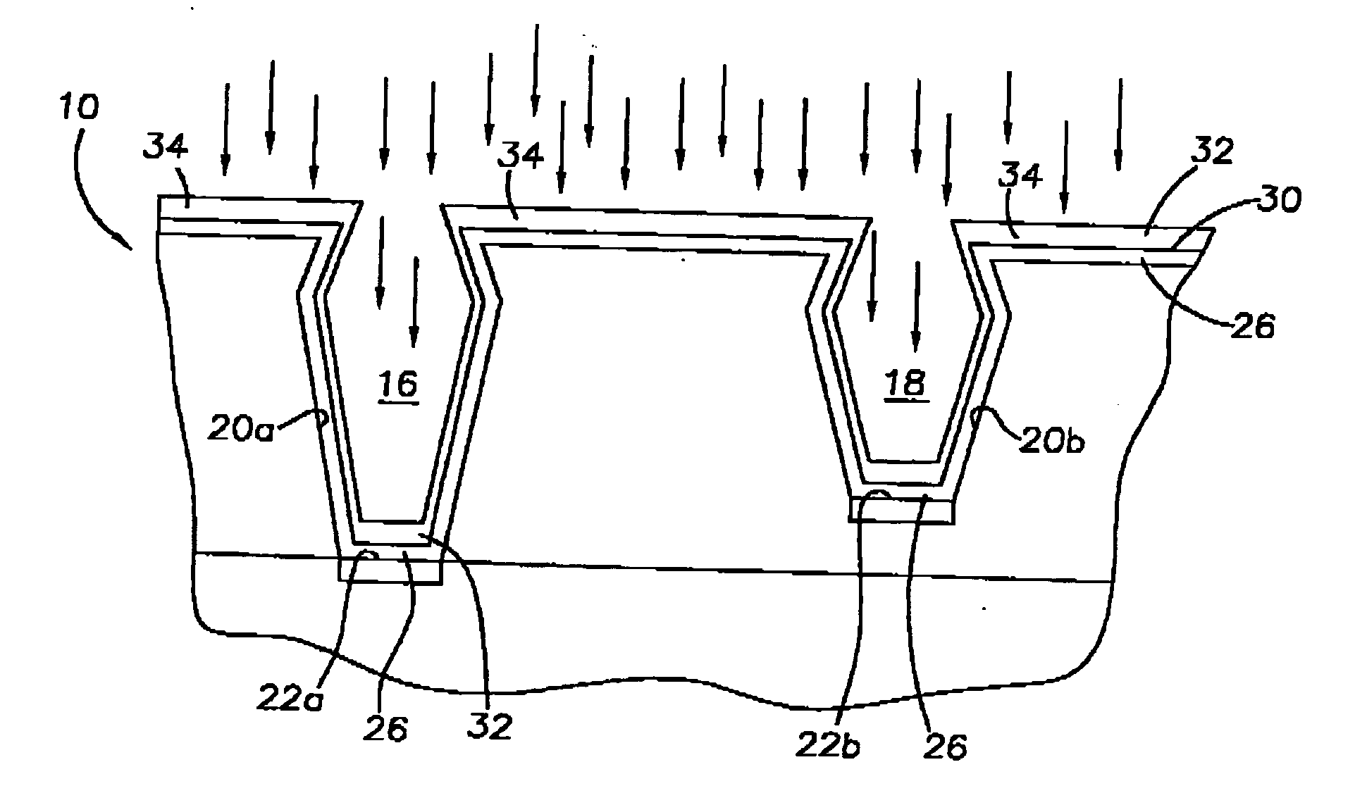
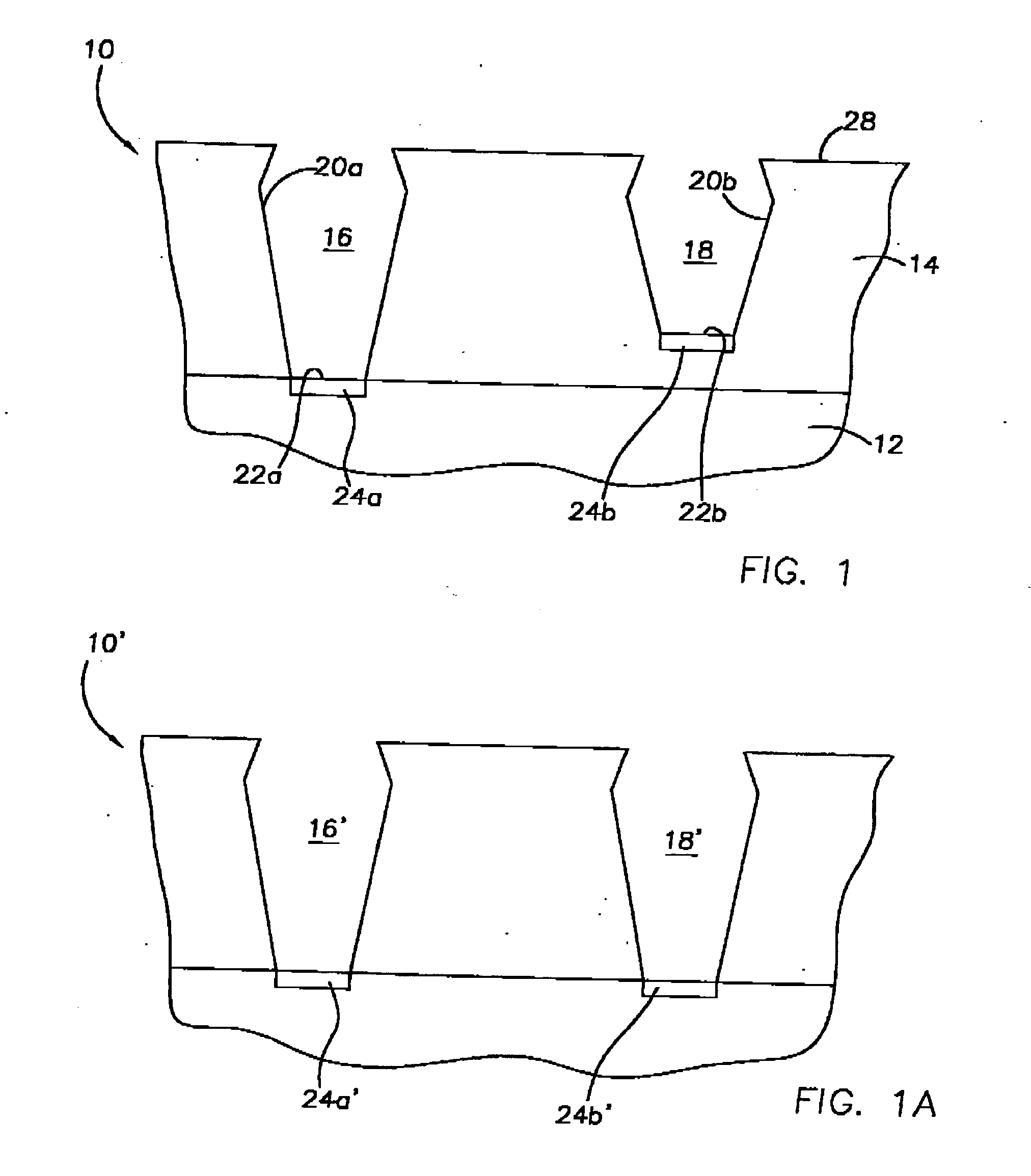
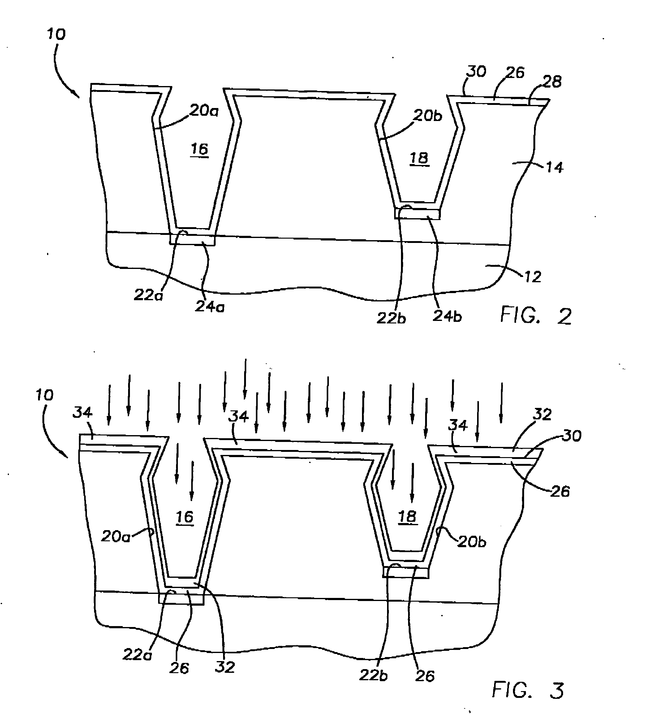
[0020] The invention will be described generally with reference to the drawings for the purpose of illustrating the present preferred embodiments only and not for purposes of limiting the same. The figures illustrate processing steps for use in the fabrication of semiconductor devices in accordance with the present invention. It should be readily apparent that the processing steps are only a portion of the entire fabrication process.

[0021] In the context of the current application, the term “semiconductor substrate” or “semiconductive substrate” or “semiconductive wafer fragment” or “wafer fragment” or “wafer” will be understood to mean any construction comprising semiconductor material, including but not limited to bulk semiconductive materials such as a semiconductor wafer (either alone or in assemblies comprising other materials thereon), and semiconductive material layers (either alone or in assemblies comprising other materials). The term “substrate” refers to any supporting s...


PUM


Abstract

Methods of electroless filling electrically different features such as contact openings to form interconnects and conductive contacts, and semiconductor devices, dies, and systems that incorporate the interconnects and contacts are disclosed. The contact openings are electrically shorted together with a selective material, a nucleation layer is selectively deposited onto the area to be plated (e.g., the base of the opening), and a conductive material is electroless plated onto the nucleation layer to fill the opening. The process achieves substantially simultaneous filling of openings having different surface potentials at an about even rate.

Description

FIELD OF THE INVENTION [0001] The invention relates generally to semiconductor processing methods of forming contacts and other features, and more particularly to processes for filling electrically different contacts or other features at an even rate with electroless deposited metals. BACKGROUND OF THE INVENTION [0002] In the fabrication of semiconductor devices, contact holes and other features that are formed on a substrate are filled with a conductive material to provide contacts and other circuitry. Electroless plating techniques are used to deposit copper, silver, platinum, and other conductive materials to fill openings. [0003] A typical plating process to fill a contact opening involves depositing a seed layer (e.g., copper) into a barrier layer formed over the substrate within the opening, and plating a layer of metal (e.g., copper) onto the substrate by applying an electrical potential between the seed layer and another electrode in the presence of an electroless solution c...

Claims


Application Information

Patent Timeline
Patent Type & Authority Applications(United States)
IPC IPC(8): H01L21/44
CPCH01L21/76879H01L21/288
Inventor COLLINS, DALE W.KLEIN, RITA J.
Owner MICRON TECH INC
Why Eureka
Try Eureka